SNVSBY3A November 2020 – April 2021 TLV840-Q1
PRODUCTION DATA
- 1 Features
- 2 Applications
- 3 Description
- 4 Revision History
- 5 Device Comparison
- 6 Pin Configuration and Functions
- 7 Specifications
- 8 Detailed Description
- 9 Application and Implementation
- 10Power Supply Recommendations
- 11Layout
- 12Device and Documentation Support
- 13Mechanical, Packaging, and Orderable Information
9.2.2 Application Curve: Adjusting Output Reset Delay on TLV840EVM
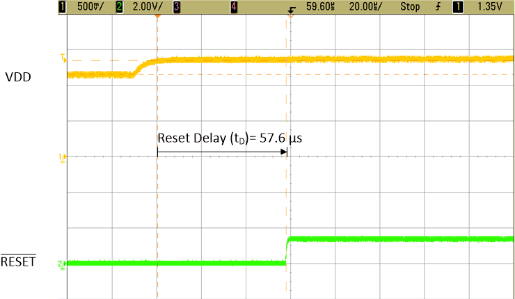
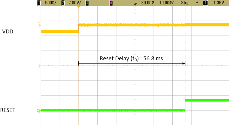
These application curves are taken with the TLV840EVM and they display a change in reset delay time with different capacitor values. The output reset delay time was designed with the ease of programability for the customer. Figure 9-3 displays an output reset delay time of 57.6 μs with no capacitor on the CT pin. Figure 9-4 and Figure 9-5 have output reset delay times of 5.42 ms and 56.8 ms, respectively. Both the output delay times and capacitors used resulted in an order of magnitude difference. Please see the TLV840EVM User Guide for more information.
 Figure 9-3 TLV840EVM
RESET Time Delay (tD) with No Capacitor
 Figure 9-5 TLV840EVM
RESET Time Delay (tD) with 0.1-µF Capacitor
 Figure 9-4 TLV840EVM
RESET Time Delay (tD) with 0.01-µF Capacitor