ZHCS493B October 2011 – April 2016 TLV717P
PRODUCTION DATA.
7 Detailed Description
7.1 Overview
The TLV717P belongs to a new family of next-generation value low-dropout (LDO) regulators. These devices consume low quiescent current and deliver excellent line and load transient performance. These characteristics, combined with low noise, very good PSRR with little (VIN – VOUT) headroom, make this family of devices ideal for RF portable applications.
This family of regulators offers current foldback. Device operating junction temperature is –40°C to 85°C.
7.3 Feature Description
7.3.1 Internal Current Limit
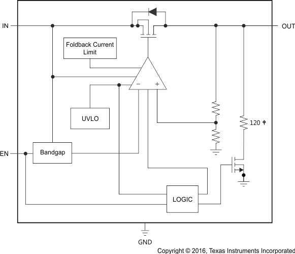
The TLV717P has an internal foldback current limit that helps to protect the regulator during fault conditions. The current supplied by the device is gradually throttled down as the output voltage decreases. When the output is shorted, the LDO supplies a typical current of 40 mA. Output voltage is not regulated when the device is in current limit, and is VOUT = ILIMIT × RLOAD. The advantage of foldback current limit is that the ILIMIT value is less than the fixed current limit. Therefore, the power that the PMOS pass transistor dissipates [(VIN – VOUT) × ILIMIT] is much less.
The TLV717P PMOS pass element has a built-in body diode that conducts current when the voltage at OUT exceeds the voltage at IN. This current is not limited, so if extended reverse voltage operation is anticipated, external limiting to 5% of the rated output current is recommended.
7.3.2 Shutdown
The enable pin (EN) is active high. The device is enabled when the voltage at the EN pin goes above 0.9 V. This relatively lower voltage value required to turn the LDO on can be exploited to power the LDO with a GPIO of recent processors whose GPIO logic 1 voltage level is lower than traditional microcontrollers. The device is turned off when the EN pin is held at less than 0.4 V. When shutdown capability is not required, EN can be connected to the IN pin.
7.3.3 Undervoltage Lockout (UVLO)
The TLV717P uses an undervoltage lockout circuit (UVLO = 1.6 V) to keep the output shut off until the internal circuitry operates properly.
7.4 Device Functional Modes
7.4.1 Normal Operation
The device regulates to the nominal output voltage under the following conditions:
- The input voltage has previously exceeded the UVLO rising voltage and has not decreased below the UVLO falling threshold.
- The input voltage is greater than the nominal output voltage added to the dropout voltage.
- The enable voltage has previously exceeded the enable rising threshold voltage and not decreased below the enable falling threshold.
- The output current is less than the current limit.
7.4.2 Dropout Operation
If the input voltage is lower than the nominal output voltage plus the specified dropout voltage, but all other conditions are met for normal operation, the device operates in dropout mode. In this condition, the output voltage is the same the input voltage minus the dropout voltage. The transient performance of the device is significantly degraded because the pass device is in a triode state and no longer controls the current through the LDO. Line or load transients in dropout may result in large output voltage deviations.
7.4.3 Disabled
The device is disabled under the following conditions:
- The input voltage is less than the UVLO falling voltage, or has not yet exceeded the UVLO rising threshold.
- The enable voltage is less than the enable falling threshold voltage or has not yet exceeded the enable rising threshold.
When the device is disabled, the active pulldown resistor discharges the output.
Table 1 lists the conditions that lead to the different modes of operation.
Table 1. Device Functional Mode Comparison
| OPERATING MODE | PARAMETER | ||
|---|---|---|---|
| VIN | VEN | IOUT | |
| Normal mode | VIN > VOUT(nom) + VDO
and VIN > UVLORISE |
VEN > VEN(HI) | IOUT < ILIM |
| Dropout mode | UVLORISE < VIN < VOUT(nom) + VDO | VEN > VEN(HI) | IOUT < ILIM |
| Disabled mode (any true condition disables the device) |
VIN < UVLOFALL | VEN < VEN(LO) | — |
