ZHCS493B October   2011  – April 2016 TLV717P

PRODUCTION DATA.  

  1. 特性
  2. 应用
  3. 说明
  4. 修订历史记录
  5. Pin Configuration and Functions
  6. Specifications
    1. 6.1 Absolute Maximum Ratings
    2. 6.2 ESD Ratings
    3. 6.3 Recommended Operating Conditions
    4. 6.4 Thermal Information
    5. 6.5 Electrical Characteristics
    6. 6.6 Typical Characteristics
  7. Detailed Description
    1. 7.1 Overview
    2. 7.2 Functional Block Diagram
    3. 7.3 Feature Description
      1. 7.3.1 Internal Current Limit
      2. 7.3.2 Shutdown
      3. 7.3.3 Undervoltage Lockout (UVLO)
    4. 7.4 Device Functional Modes
      1. 7.4.1 Normal Operation
      2. 7.4.2 Dropout Operation
      3. 7.4.3 Disabled
  8. Application and Implementation
    1. 8.1 Application Information
    2. 8.2 Typical Application
      1. 8.2.1 Design Requirements
      2. 8.2.2 Detailed Design Procedure
        1. 8.2.2.1 Input and Output Capacitor Requirements
        2. 8.2.2.2 Dropout Voltage
        3. 8.2.2.3 Transient Response
      3. 8.2.3 Application Curves
  9. Power Supply Recommendations
  10. 10Layout
    1. 10.1 Layout Guidelines
    2. 10.2 Layout Example
    3. 10.3 Power Dissipation
  11. 11器件和文档支持
    1. 11.1 器件支持
      1. 11.1.1 开发支持
        1. 11.1.1.1 评估模块
      2. 11.1.2 器件命名规则
    2. 11.2 文档支持
      1. 11.2.1 相关文档
    3. 11.3 社区资源
    4. 11.4 商标
    5. 11.5 静电放电警告
    6. 11.6 Glossary
  12. 12机械封装和可订购信息

封装选项

机械数据 (封装 | 引脚)
散热焊盘机械数据 (封装 | 引脚)
订购信息

10 Layout

10.1 Layout Guidelines

Input and output capacitors should be placed as close to the device pins as possible. To improve AC performance (such as PSRR, output noise, and transient response), TI recommends designing the board with separate ground planes for VIN and VOUT, with the ground plane connected only at the device GND pin. In addition, the output capacitor ground connection should be connected directly to the device GND pin. High ESR capacitors may degrade PSRR performance.

10.2 Layout Example
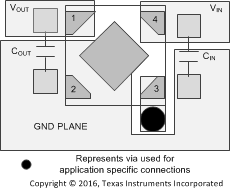
TLV717P dqn_layout_bvs153.gif Figure 18. Recommended Layout Example

10.3 Power Dissipation

The ability to remove heat from the die is different for each package type, presenting different considerations in the printed-circuit board (PCB) layout. The PCB area around the device that is free of other components moves the heat from the device to ambient air. Performance data for JEDEC-low and high-K boards are given in Thermal Information. Using heavier copper increases the effectiveness in removing heat from the device. The addition, plated through-holes to heat-dissipating layers also improves heatsink effectiveness.

Power dissipation depends on input voltage and load conditions. Power dissipation (PD) is equal to the product of the output current and the voltage drop across the output pass element, as shown in Equation 1.

Equation 1. PD = (VIN – VOUT) × IOUT