ZHCSBE7D August 2013 – July 2019 TLV702-Q1
PRODUCTION DATA.
- 1 特性
- 2 应用
- 3 说明
- 4 修订历史记录
- 5 Pin Configuration and Functions
- 6 Specifications
- 7 Detailed Description
- 8 Application and Implementation
- 9 Power Supply Recommendations
- 10Layout
- 11器件和文档支持
- 12机械、封装和可订购信息
封装选项
机械数据 (封装 | 引脚)
散热焊盘机械数据 (封装 | 引脚)
订购信息
5 Pin Configuration and Functions
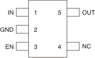
DDC and DBV Package
5-pin SOT
Top View

DSE Package
6-Pin WSON
Top View

Pin Functions
| PIN | I/O | DESCRIPTION | ||
|---|---|---|---|---|
| NAME | DDC, DBV
(SOT) |
DSE
(WSON) |
||
| IN | 1 | 1 | I | Input pin. A small, 1-μF ceramic capacitor is recommended from this pin to ground to assure stability and good transient performance. See Input and Output Capacitor Requirements in the Application Information section for more details. |
| GND | 2 | 2 | — | Ground pin |
| EN | 3 | 6 | I | Enable pin. Driving EN over 0.9 V turns on the regulator. Driving EN below 0.4 V puts the regulator into shutdown mode and reduces operating current to 1 μA, nominal. |
| NC | 4 | 4, 5 | — | No connection. Tie this pin to ground to improve thermal dissipation. |
| OUT | 5 | 3 | O | Regulated output voltage pin. A small, 1-μF ceramic capacitor is needed from this pin to ground for stability. See Input and Output Capacitor Requirements in the Application Information section for more details. |