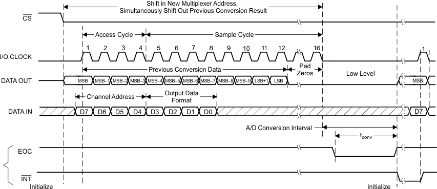
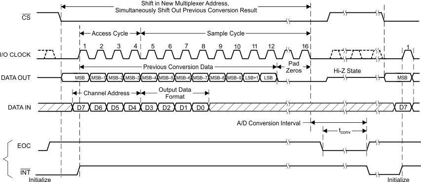
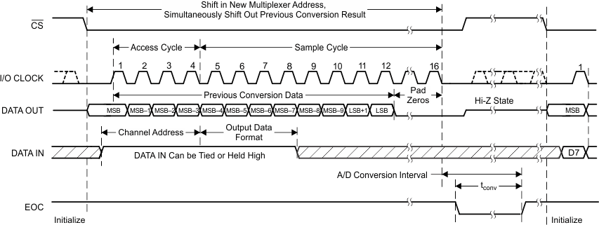
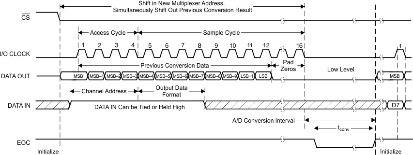
6 Specifications
6.1 Absolute Maximum Ratings
over operating free-air temperature range (unless otherwise noted)(1)
|
MIN |
MAX |
UNIT |
| VCC |
Supply voltage(2) |
–0.5 |
6.5 |
V |
| VI |
Input voltage (any input) |
–0.3 |
VCC + 0.3 |
V |
| VO |
Output voltage |
–0.3 |
VCC + 0.3 |
V |
| Vref+ |
Positive reference voltage |
–0.3 |
VCC + 0.3 |
V |
| Vref– |
Negative reference voltage |
–0.3 |
VCC + 0.3 |
V |
| II |
Peak input current (any input) |
–20 |
20 |
mA |
|
Peak total input current (all inputs) |
–30 |
30 |
mA |
| TJ |
Operating virtual junction temperature |
–40 |
150 |
°C |
| TA |
Operating free-air temperature |
–40 |
85 |
°C |
|
Lead temperature 1.6 mm (1/16 inch) from the case for 10 s |
|
260 |
°C |
| Tstg |
Storage temperature |
–65 |
150 |
°C |
(1) Stresses beyond those listed under Absolute Maximum Ratings may cause permanent damage to the device. These are stress ratings only, and functional operation of the device at these or any other conditions beyond those indicated under Recommended Operating Conditions is not implied. Exposure to absolute-maximum-rated conditions for extended periods may affect device reliability.
(2) All voltage values are with respect to the GND terminal with REF– and GND wired together (unless otherwise noted).
6.2 ESD Ratings
|
VALUE |
UNIT |
| V(ESD) |
Electrostatic discharge |
Human body model (HBM), per ANSI/ESDA/JEDEC JS-001(1) |
±2000 |
V |
| Charged-device model (CDM), per JEDEC specification JESD22-C101(2) |
±500 |
(1) JEDEC document JEP155 states that 500-V HBM allows safe manufacturing with a standard ESD control process.
(2) JEDEC document JEP157 states that 250-V CDM allows safe manufacturing with a standard ESD control process.
6.3 Recommended Operating Conditions
|
MIN |
NOM |
MAX |
UNIT |
| VCC |
Supply voltage |
2.7 |
|
5.5 |
V |
|
I/O CLOCK frequency |
VCC = 4.5 V to 5.5 V |
16-bit I/O |
0.01 |
|
15 |
MHz |
| 12-bit I/O |
0.01 |
|
15 |
| 8-bit I/O |
0.01 |
|
15 |
| VCC = 2.7 to 3.6 V |
0.01 |
|
10 |
|
Tolerable clock jitter, I/O CLOCK |
VCC = 4.5 V to 5.5 V |
|
|
0.38 |
ns |
|
Aperature jitter |
VCC = 4.5 V to 5.5 V |
|
100 |
|
ps |
|
Analog input voltage(1) |
VCC = 4.5 V to 5.5 V |
0 |
|
REF+ – REF– |
V |
| VCC = 3 V to 3.6 V |
0 |
|
REF+ – REF– |
| VCC = 2.7 V to 3 V |
0 |
|
REF+ – REF– |
| VIH |
High-level control input voltage |
VCC = 4.5 V to 5.5 V |
2 |
|
|
V |
| VCC = 2.7 V to 3.6 V |
2.1 |
|
|
| VIL |
Low-level control input voltage |
VCC = 4.5 V to 5.5 V |
|
|
0.8 |
V |
| VCC = 2.7 V to 3.6 V |
|
|
0.6 |
| TA |
Operating free-air temperature |
–40 |
|
85 |
°C |
(1) Analog input voltages greater than the voltage applied to REF+ convert as all ones (111111111111), while input voltages less than the voltage applied to REF– convert as all zeros (000000000000).
6.4 Thermal Information
| THERMAL METRIC(1) |
TLV2556 |
UNIT |
| DW (SOIC) |
PW (TSSOP) |
| 20 PINS |
20 PINS |
| RθJA |
Junction-to-ambient thermal resistance |
66.0 |
88.1 |
°C/W |
| RθJC(top) |
Junction-to-case (top) thermal resistance |
31.4 |
21.6 |
°C/W |
| RθJB |
Junction-to-board thermal resistance |
33.7 |
40.4 |
°C/W |
| ψJT |
Junction-to-top characterization parameter |
7.4 |
0.8 |
°C/W |
| ψJB |
Junction-to-board characterization parameter |
33.3 |
39.7 |
°C/W |
| RθJC(bot) |
Junction-to-case (bottom) thermal resistance |
N/A |
N/A |
°C/W |
(1) For more information about traditional and new thermal metrics, see the
Semiconductor and IC Package Thermal Metrics application report,
SPRA953.
6.5 Electrical Characteristics
over recommended operating free-air temperature range, when VCC = 5 V: VREF+ = 5 V, I/O CLOCK frequency = 15 MHz,
when VCC = 2.7 V: VREF+ = 2.5 V, I/O CLOCK frequency = 10 MHz (unless otherwise noted)
| PARAMETER |
TEST CONDITIONS |
MIN |
TYP(1) |
MAX |
UNIT |
| VOH |
High-level output voltage |
VCC = 4.5 V, IOH = –1.6 mA
VCC = 2.7 V, IOH = –0.2 mA |
30 pF |
2.4 |
|
|
V |
VCC = 4.5 V, IOH = –20 μA
VCC = 2.7 V, IOH = –20 μA |
VCC – 0.1 |
|
|
| VOL |
Low-level output voltage |
VCC = 4.5 V, IOL = 1.6 mA
VCC = 2.7 V, IOL = 0.8 mA |
30 pF |
|
|
0.4 |
V |
VCC = 4.5 V, IOL = 20 μA
VCC = 2.7 V, IOL = 20 μA |
|
|
0.1 |
| IOZ |
High-impedance OFF-state output current |
VO = VCC, CS = VCC |
|
1 |
2.5 |
μA |
| VO = 0 V, CS = VCC |
|
–1 |
–2.5 |
| ICC |
Operating supply current |
CS = 0 V, External reference |
VCC = 5 V |
|
|
1.2 |
mA |
| VCC = 2.7 V |
|
|
0.9 |
| CS = 0 V, Internal reference |
VCC = 5 V |
|
|
3 |
mA |
| VCC = 2.7 V |
|
|
2.4 |
| ICC(PD) |
Power-down current |
For all digital inputs, 0 ≤ VI ≤ 0.5 V or VI ≥ VCC – 0.5 V, I/O CLOCK = 0 V |
Software power down |
Ext. Ref |
|
0.1 |
1 |
μA |
| Int. Ref |
|
0.1 |
1 |
| Auto power down |
Ext. Ref |
|
0.1 |
10 |
| Int. Ref |
|
|
1800 |
| IIH |
High-level input current |
VI = VCC |
|
0.005 |
2.5 |
μA |
| IIL |
Low-level input current |
VI = 0 V |
|
–0.005 |
–2.5 |
μA |
| Ilkg |
Selected channel leakage current |
Selected channel at VCC ,
Unselected channel at 0 V |
|
|
1 |
μA |
Selected channel at 0 V,
Unselected channel at VCC |
|
|
–1 |
| fOSC |
Internal oscillator frequency |
VCC = 4.5 V to 5.5 V |
3.27 |
|
|
MHz |
| VCC = 2.7 V to 3.6 V |
2.56 |
|
|
| tconvert |
Conversion time
(13.5 × (1/fOSC) + 25 ns) |
VCC = 4.5 V to 5.5 V |
|
|
4.15 |
μs |
| VCC = 2.7 V to 3.6 V |
|
|
5.54 |
|
Internal oscillator frequency switch over voltage |
|
3.6 |
|
4.1 |
V |
| Zi |
Input impedance(2) |
Analog inputs |
VCC = 4.5 V |
|
|
600 |
Ω |
| VCC = 2.7 V |
|
|
500 |
| Ci |
Input capacitance |
Analog inputs |
|
|
45 |
55 |
pF |
| Control inputs |
|
|
5 |
15 |
(1) All typical values are at VCC = 5 V, TA = 25°C.
(2) The switch resistance is very nonlinear and varies with input voltage and supply voltage. This is the worst case.
6.6 External Reference Specifications
See (2)
| PARAMETER |
TEST CONDITIONS |
MIN |
TYP(1) |
MAX |
UNIT |
| VREF– |
Reference input voltage, REF– |
VCC = 4.5 V to 5.5 V |
–0.1 |
0 |
0.1 |
V |
| VCC = 2.7 V to 3.6 V |
–0.1 |
0 |
0.1 |
| VREF+ |
Reference input voltage, REF+ |
VCC = 4.5 V to 5.5 V |
2 |
|
VCC |
V |
| VCC = 2.7 V to 3.6 V |
2 |
|
VCC |
|
External reference input voltage difference (REF+ – REF–) |
VCC = 4.5 V to 5.5 V |
1.9 |
|
VCC |
V |
| VCC = 2.7 V to 3.6 V |
1.9 |
|
VCC |
| IREF |
External reference supply current |
CS = 0 V |
VCC = 4.5 V to 5.5 V |
|
|
1 |
mA |
| VCC = 2.7 V to 3.6 V |
|
|
0.7 |
| ZREF |
Reference input impedance |
VCC = 5 V |
Static |
1 |
|
|
MΩ |
| During sampling or conversion |
6 |
|
9 |
kΩ |
| VCC = 2.7 V |
Static |
1 |
|
|
MΩ |
| During sampling or conversion |
6 |
|
9 |
kΩ |
(1) All typical values are at VCC = 5 V, TA = 25°C.
(2) Add a 0.1-μF capacitor between REF+ and REF– pins when external reference is used.
6.7 Internal Reference Specifications
See (1)(2)(3)
| PARAMETER |
TEST CONDITIONS |
MIN |
TYP(4) |
MAX |
UNIT |
| VREF– |
Reference input voltage, REF– |
VCC = 2.7 V to 5.5 V, REF- = Analog GND |
|
0 |
|
V |
|
Internal reference delta voltage, (REF+ – REF–) |
VCC = 5.5 V |
Internal 4.096 V selected |
3.95 |
4.065 |
4.25 |
V |
| Internal 2.048 V selected |
1.95 |
2.019 |
2.1 |
| VCC = 2.7 V |
Internal 2.048 V selected |
1.95 |
2.019 |
2.1 |
|
Internal reference start-up time |
VCC = 5 V |
With 10-µF load |
|
20 |
|
ms |
| VCC = 2.7 V |
|
20 |
|
|
Internal reference temperature coefficient |
VCC = 2.7 V to 5.5 V |
|
±50 |
|
ppm/°C |
(1) Add a 0.1-μF capacitor between REF+ and REF– pins when external reference is used.
(2) Add a 0.1-μF capacitor between REF+ and REF– pins.
(3) REF- must be connected to analog GND (the ground of the ADC).
(4) All typical values are at VCC = 5 V, TA = 25°C.
6.8 Operating Characteristics
over recommended operating free-air temperature range, when VCC = 5 V: VREF+ = 5 V, I/O CLOCK frequency = 15 MHz,
when VCC = 2.7 V: VREF+ = 2.5 V, I/O CLOCK frequency = 10 MHz (unless otherwise noted)
| PARAMETER |
TEST CONDITIONS |
MIN |
TYP(1) |
MAX |
UNIT |
| INL |
Integral linearity error(3) |
|
–1 |
|
1 |
LSB |
| DNL |
Differential linearity error |
|
–1 |
|
1 |
LSB |
| EO |
Offset error(4) |
See (2) |
–2 |
|
2 |
mV |
| EG |
Gain error(4) |
See (2) |
–3 |
|
3 |
mV |
| ET |
Total unadjusted error(5) |
|
|
±1.5 |
|
LSB |
|
Self-test output code(6) |
Address data input = 1011 |
|
2048 |
|
|
| Address data input = 1100 |
|
0 |
|
| Address data input = 1101 |
|
4095 |
|
(1) All typical values are at VCC = 5 V, TA = 25°C.
(2) Analog input voltages greater than the voltage applied to REF+ convert as all ones (111111111111), while input voltages less than the voltage applied to REF– convert as all zeros (000000000000).
(3) Linearity error is the maximum deviation from the best straight line through the A/D transfer characteristics.
(4) Gain error is the difference between the actual midstep value and the nominal midstep value in the transfer diagram at the specified gain point after the offset error has been adjusted to zero. Offset error is the difference between the actual midstep value and the nominal midstep value at the offset point.
(5) Total unadjusted error comprises linearity, zero-scale errors, and full-scale errors.
(6) Both the input address and the output codes are expressed in positive logic.
6.9 Timing Requirements, VREF+ = 5 V
over recommended operating free-air temperature range,
VREF+ = 5 V, I/O CLOCK frequency = 15 MHz, VCC = 5 V, Load = 25 pF (unless otherwise noted)
|
MIN |
MAX |
UNIT |
| tw1 |
Pulse duration I/O CLOCK high or low |
26.7 |
100000 |
ns |
| tsu1 |
Set-up time DATA IN valid before I/O CLOCK rising edge (see Figure 47) |
12 |
|
ns |
| th1 |
Hold time DATA IN valid after I/O CLOCK rising edge (see Figure 47) |
0 |
|
ns |
| tsu2 |
Setup time CS low before first rising I/O CLOCK edge(2) (see Figure 48) |
25 |
|
ns |
| th2 |
Hold time CS pulse duration high time (see Figure 48) |
100 |
|
ns |
| th3 |
Hold time CS low after last I/O CLOCK falling edge (see Figure 48) |
0 |
|
ns |
| th4 |
Hold time DATA OUT valid after I/O CLOCK falling edge (see Figure 49) |
2 |
|
ns |
| th5 |
Hold time CS high after EOC rising edge when CS is toggled (see Figure 52) |
0 |
|
ns |
| th6 |
Hold time CS high after INT falling edge (seeFigure 52) |
0 |
|
ns |
| th7 |
Hold time I/O CLOCK low after EOC rising edge or INT falling edge when CS is held low (seeFigure 53) |
10 |
|
ns |
| td1 |
Delay time CS falling edge to DATA OUT valid (MSB or LSB) (see Figure 46) |
Load = 25 pF |
|
28 |
ns |
| Load = 10 pF |
|
20 |
| td2 |
Delay time CS rising edge to DATA OUT high impedance (see Figure 46) |
|
10 |
ns |
| td3 |
Delay time I/O CLOCK falling edge to next DATA OUT bit valid (see Figure 49) |
2 |
20 |
ns |
| td4 |
Delay time last I/O CLOCK falling edge to EOC falling edge (seeFigure 50) |
|
55 |
ns |
| td5 |
Delay time last I/O CLOCK falling edge to CS falling edge to abort conversion |
|
1.5 |
μs |
| td6 |
Delay time last I/O CLOCK falling edge to INT falling edge (see Figure 50) |
|
tconvert(max) |
ns |
| td7 |
Delay time EOC rising edge or INT falling edge to DATA OUT valid: MSB or LSB 1st (see Figure 51) |
|
4 |
ns |
| td9 |
Delay time I/O CLOCK high to INT rising edge when CS is held low (see Figure 53) |
1 |
28 |
ns |
| tt1 |
Transition time I/O CLOCK(2) (see Figure 49) |
|
1 |
μs |
| tt2 |
Transition time DATA OUT (see Figure 49) |
|
5 |
ns |
| tt3 |
Transition time INT/EOC, CL = 7 pF (see Figure 50 and Figure 51) |
|
2.4 |
ns |
| tt4 |
Transition time DATA IN, CS |
|
10 |
μs |
| tcycle |
Total cycle time (sample, conversion and delays)(2) |
|
See (1) |
μs |
| tsample |
Channel acquisition time (sample) at 1 kΩ(2)
(see Figure 1 through Figure 6) |
Source impedance = 25 Ω |
600 |
|
ns |
| Source impedance = 100 Ω |
650 |
|
| Source impedance = 500 Ω |
700 |
|
| Source impedance = 1 kΩ |
1000 |
|
(1) t
convert(max) + I/O CLOCK period (8/12/16 CLKs)
(2)
(2) I/O CLOCK period = 8 × [1/(I/O CLOCK frequency)] or 12 × [1/(I/O CLOCK frequency)] or 16 × [1/(I/O CLOCK frequency)], depending on I/O format selected
6.10 Timing Requirements, VREF+ = 2.5 V
over recommended operating free-air temperature range,
VREF+ = 2.5 V, I/O CLOCK frequency = 10 MHz, VCC = 2.7 V, Load = 25 pF (unless otherwise noted)
|
MIN |
MAX |
UNIT |
| tw1 |
Pulse duration I/O CLOCK high or low |
40 |
100000 |
ns |
| tsu1 |
Set-up time DATA IN valid before I/O CLOCK rising edge (see Figure 47) |
22 |
|
ns |
| th1 |
Hold time DATA IN valid after I/O CLOCK rising edge (see Figure 47) |
0 |
|
ns |
| tsu2 |
Setup time CS low before first rising I/O CLOCK edge(2) (see Figure 48) |
33 |
|
ns |
| th2 |
Hold time CS pulse duration high time (see Figure 48) |
100 |
|
ns |
| th3 |
Hold time CS low after last I/O CLOCK falling edge (see Figure 48) |
0 |
|
ns |
| th4 |
Hold time DATA OUT valid after I/O CLOCK falling edge (see Figure 49) |
2 |
|
ns |
| th5 |
Hold time CS high after EOC rising edge when CS is toggled (see Figure 52) |
0 |
|
ns |
| th6 |
Hold time CS high after INT falling edge (see Figure 52) |
0 |
|
ns |
| th7 |
Hold time I/O CLOCK low after EOC rising edge or INT falling edge when CS is held low (see Figure 53) |
10 |
|
ns |
| td1 |
Delay time CS falling edge to DATA OUT valid (MSB or LSB) (see Figure 46) |
Load = 25 pF |
|
30 |
ns |
| Load = 10 pF |
|
22 |
| td2 |
Delay time CS rising edge to DATA OUT high impedance (see Figure 46) |
|
10 |
ns |
| td3 |
Delay time I/O CLOCK falling edge to next DATA OUT bit valid (see Figure 49) |
2 |
33 |
ns |
| td4 |
Delay time last I/O CLOCK falling edge to EOC falling edge (see Figure 50) |
|
75 |
ns |
| td5 |
Delay time last I/O CLOCK falling edge to CS falling edge to abort conversion |
|
1.5 |
μs |
| td6 |
Delay time last I/O CLOCK falling edge to INT falling edge (see Figure 50) |
|
tconvert(max) |
ns |
| td7 |
Delay time EOC rising edge or INT falling edge to DATA OUT valid: MSB or LSB 1st (see Figure 51) |
|
20 |
ns |
| td9 |
Delay time I/O CLOCK high to INT rising edge when CS is held low (see Figure 53) |
|
55 |
ns |
| tt1 |
Transition time I/O CLOCK(2) (see Figure 49) |
|
1 |
μs |
| tt2 |
Transition time DATA OUT (see Figure 49) |
|
5 |
ns |
| tt3 |
Transition time INT/EOC, CL = 7 pF (see Figure 50 and Figure 51) |
|
4 |
ns |
| tt4 |
Transition time DATA IN, CS |
|
10 |
μs |
| tcycle |
Total cycle time (sample, conversion and delays)(2) |
|
See (1) |
μs |
| tsample |
Channel acquisition time (sample), at 1 kΩ(2)
(see Figure 1 through Figure 6) |
Source impedance = 25 Ω |
800 |
|
ns |
| Source impedance = 100 Ω |
850 |
|
| Source impedance = 500 Ω |
1000 |
|
| Source impedance = 1 kΩ |
1600 |
|
(1) t
convert(max) + I/O CLOCK period (8/12/16 CLKs)
(2)
(2) I/O CLOCK period = 8 × [1/(I/O CLOCK frequency)] or 12 × [1/(I/O CLOCK frequency)] or 16 × [1/(I/O CLOCK frequency)], depending on I/O format selected
The host must configure CFGR2 before valid device conversions can begin. This can be accessed through command 1111. This can be done using eight, twelve, or sixteen I/O CLOCK clocks. (A minimum of eight is required to fully program CFGR2.)
After CFGR2 is configured, the following cycle configures CFGR1 and a valid sample or conversion is performed. CS can be held low for each remaining cycle. First valid conversion output data is available on the third cycle after power up.
To remove the device from default mode, CFGR2 – D0 must be reset to 0. Valid sample or convert cycles can resume on the cycle following the CFGR2 configuration.
6.11 Typical Characteristics
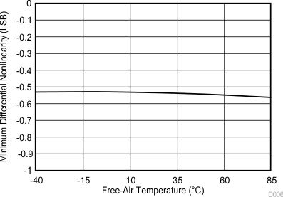
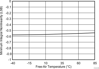
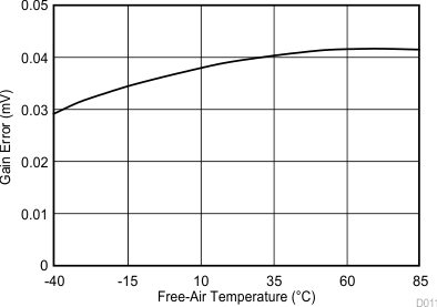
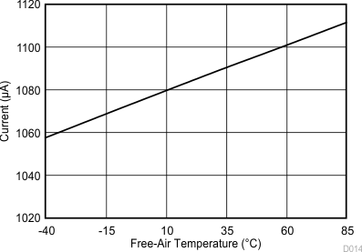
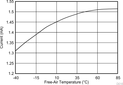
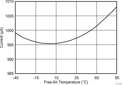
VREF– = 0 V

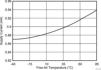
| VCC = 3.3 V |
VREF+ = 2.048 V |
VREF- = 0 V |
| I/O clock = 10 MHz |
fSAMP = 150 kSPS |
|
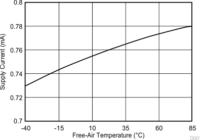
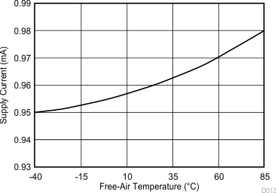
Figure 10. Supply Current vs Free-Air Temperature

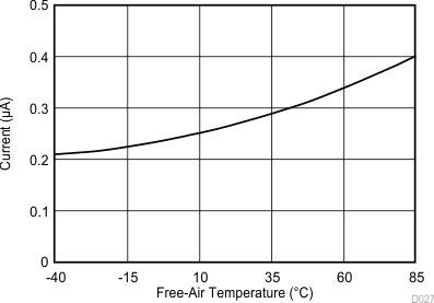
| VCC = 3.3 V |
VREF+ = 2.048 V |
VREF- = 0 V |
| I/O clock = 10 MHz |
fSAMP = 150 kSPS |
|
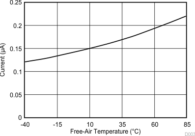
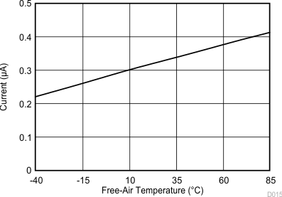
Figure 12. Software Power Down vs Free-Air Temperature

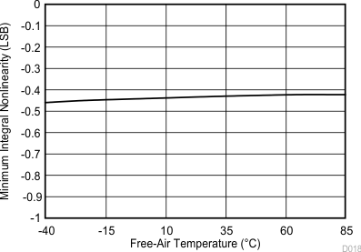
| VCC = 2.7 V |
VREF+ = 2.048 V |
VREF- = 0 V |
| I/O clock = 10 MHz |
fSAMP = 150 kSPS |
|
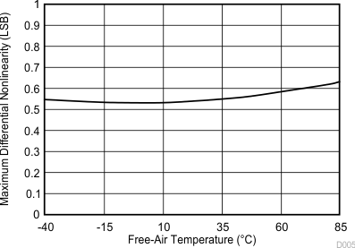
Figure 14. Maximum Differential Nonlinearity vs Free-Air Temperature

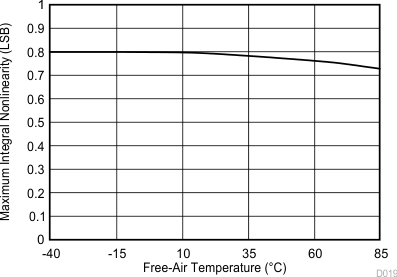
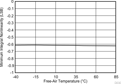
| VCC = 2.7 V |
VREF+ = 2.048 V |
VREF- = 0 V |
| I/O clock = 10 MHz |
fSAMP = 150 kSPS |
|
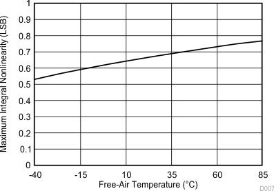
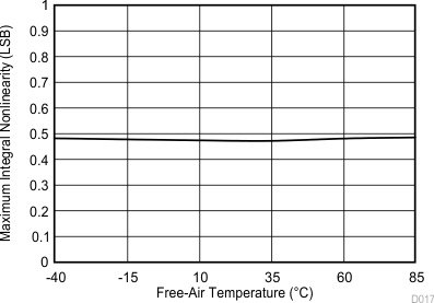
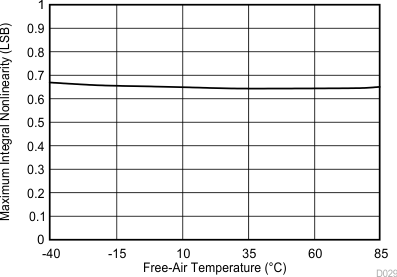
Figure 16. Maximum Integral Nonlinearity vs Free-Air Temperature

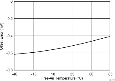
| VCC = 3.3 V |
VREF+ = 2.048 V |
VREF- = 0 V |
| I/O clock = 10 MHz |
fSAMP = 150 kSPS |
|
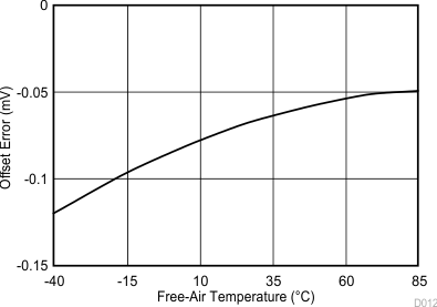
Figure 18. Offset Error vs Free-Air Temperature

| VCC = 5.5 V |
VREF+ = 4.096 V |
VREF- = 0 V |
| I/O clock = 15 MHz |
fSAMP = 200 kSPS |
|
Figure 20. Supply Current vs Free-Air Temperature

| VCC = 5.5 V |
VREF+ = 4.096 V |
VREF- = 0 V |
| I/O clock = 15 MHz |
fSAMP = 200 kSPS |
|
Figure 22. Software Power Down vs Free-Air Temperature

| VCC = 5.5 V |
VREF+ = 4.096 V |
VREF- = 0 V |
| I/O clock = 15 MHz |
fSAMP = 200 kSPS |
|
Figure 24. Maximum Differential Nonlinearity vs Free-Air Temperature

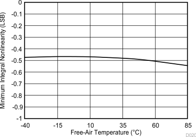
| VCC = 5.5 V |
VREF+ = 4.096 V |
VREF- = 0 V |
| I/O clock = 15 MHz |
fSAMP = 200 kSPS |
|
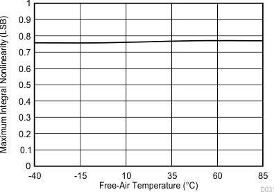
Figure 26. Maximum Integral Nonlinearity vs Free-Air Temperature

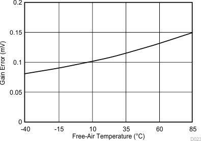
| VCC = 5.5 V |
VREF+ = 4.096 V |
VREF- = 0 V |
| I/O clock = 15 MHz |
fSAMP = 200 kSPS |
|
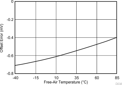
Figure 28. Offset Error vs Free-Air Temperature

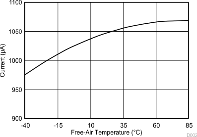
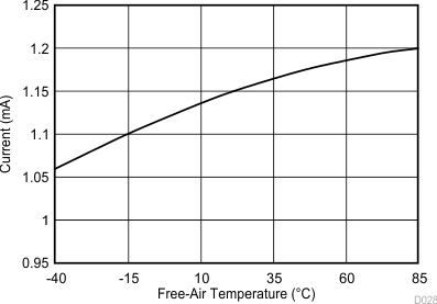
| VCC = 5.5 V |
VREF+ = 2.048 V |
VREF- = 0 V |
| I/O clock = 15 MHz |
fSAMP = 200 kSPS |
|
Figure 30. Supply Current vs Free-Air Temperature

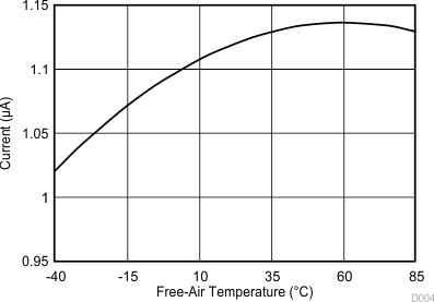
| VCC = 5.5 V |
VREF+ = 2.048 V |
VREF- = 0 V |
| I/O clock = 15 MHz |
fSAMP = 200 kSPS |
|
Figure 32. Software Power Down vs Free-Air Temperature

| VCC = 5.5 V |
VREF+ = 2.048 V |
VREF- = 0 V |
| I/O clock = 15 MHz |
fSAMP = 200 kSPS |
|
Figure 34. Maximum Differential Nonlinearity vs Free-Air Temperature

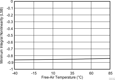
| VCC = 5.5 V |
VREF+ = 2.048 V |
VREF- = 0 V |
| I/O clock = 15 MHz |
fSAMP = 200 kSPS |
|
Figure 36. Maximum Integral Nonlinearity vs Free-Air Temperature

| VCC = 5.5 V |
VREF+ = 2.048 V |
VREF- = 0 V |
| I/O clock = 15 MHz |
fSAMP = 200 kSPS |
|
Figure 38. Offset Error vs Free-Air Temperature

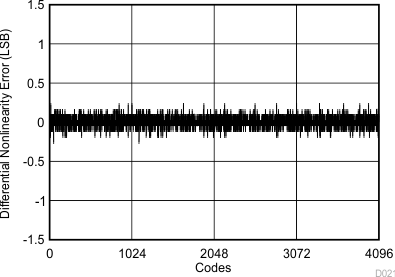
| VCC = 2.7 V |
VREF+ = 2.048 V |
VREF- = 0 V |
| I/O clock = 10 MHz |
fSAMP = 150 kSPS |
TA = 25°C |
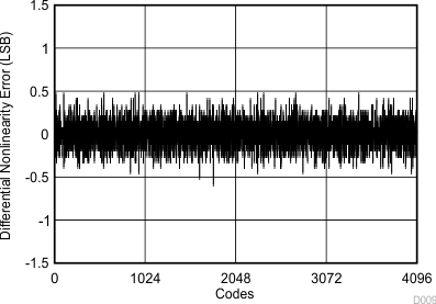
Figure 40. Differential Nonlinearity vs Digital Output Code

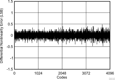
| VCC = 5.5 V |
VREF+ = 4.096 V |
VREF- = 0 V |
| I/O clock = 15 MHz |
fSAMP = 200 kSPS |
TA = 25°C |
Figure 42. Differential Nonlinearity vs Digital Output Code

| VCC = 5.5 V |
VREF+ = 2.048 V |
VREF- = 0 V |
| I/O clock = 10 MHz |
fSAMP = 200 kSPS |
TA = 25°C |
Figure 44. Differential Nonlinearity vs Digital Output Code

