ZHCSDU7C July 2015 – September 2017 TLK10031
PRODUCTION DATA.
- 1 器件概述
- 2 修订历史记录
- 3 说明
- 4 Terminal Configuration and Functions
-
5 Specifications
- 5.1 Absolute Maximum Ratings
- 5.2 ESD Ratings
- 5.3 Recommended Operating Conditions
- 5.4 Thermal Information
- 5.5 Electrical Characteristics: High Speed Side Serial Transmitter
- 5.6 Electrical Characteristics: High Speed Side Serial Receiver
- 5.7 Electrical Characteristics: Low Speed Side Serial Transmitter
- 5.8 Electrical Characteristics: Low Speed Side Serial Receiver
- 5.9 Electrical Characteristics: LVCMOS (VDDO):
- 5.10 Electrical Characteristics: Clocks
- 5.11 Timing Requirements
- 5.12 Typical Characteristics
- 6 Parametric Measurement Information
-
7 Detailed Description
- 7.1 Overview
- 7.2 Functional Block Diagrams
- 7.3
Feature Description
- 7.3.1 10GBASE-KR Transmit Data Path Overview
- 7.3.2 10GBASE-KR Receive Data Path Overview
- 7.3.3 Channel Synchronization Block
- 7.3.4 8B/10B Encoder
- 7.3.5 8B/10B Decoder
- 7.3.6 64B/66B Encoder/Scrambler
- 7.3.7 Forward Error Correction
- 7.3.8 64B/66B Decoder/Descrambler
- 7.3.9 Transmit Gearbox
- 7.3.10 Receive Gearbox
- 7.3.11 XAUI Lane Alignment / Code Gen (XAUI PCS)
- 7.3.12 Inter-Packet Gap (IPG) Characters
- 7.3.13 Clock Tolerance Compensation (CTC)
- 7.3.14 10GBASE-KR Auto-Negotiation
- 7.3.15 10GBASE-KR Link Training
- 7.3.16 10GBASE-KR Line Rate, PLL Settings, and Reference Clock Selection
- 7.3.17 10GBASE-KR Test Pattern Support
- 7.3.18 10GBASE-KR Latency
- 7.4
Device Functional Modes
- 7.4.1 10GBASE-KR Mode
- 7.4.2 1GBASE-KX Mode
- 7.4.3 General Purpose (10G) Serdes Mode Functional Description
- 7.4.4 General Purpose SERDES Receive Data Path
- 7.4.5 Channel Synchronization
- 7.4.6 8B/10B Encoder and Decoder
- 7.4.7 Lane Alignment Scheme for 8b/10b General Purpose Serdes Mode
- 7.4.8 Lane Alignment Components
- 7.4.9 Lane Alignment Operation
- 7.4.10 Line Rate, SERDES PLL Settings, and Reference Clock Selection for the General Purpose SERDES Mode
- 7.4.11 General Purpose SERDES Mode Test Pattern Support
- 7.4.12 General Purpose SERDES Mode Latency
- 7.4.13 Intelligent Switching Modes
- 7.4.14 Serial Loopback Modes
- 7.4.15 Latency Measurement Function (General Purpose SerDes Mode)
- 7.4.16 Power Down Mode
- 7.4.17 MDIO Management Interface
- 7.4.18 MDIO Protocol Timing
- 7.4.19 Clause 22 Indirect Addressing
- 7.4.20 Provisionable XAUI Clock Tolerance Compensation
- 7.5
Register Maps
- 7.5.1 Register Bit Definitions
- 7.5.2
Vendor Specific Device Registers
- 7.5.2.1 GLOBAL_CONTROL_1 (register: 0x0000) (default: 0x0610) (device address: 0x1E)
- 7.5.2.2 CHANNEL_CONTROL_1 (register: 0x0001) (default: 0x0B00) (device address: 0x1E)
- 7.5.2.3 HS_SERDES_CONTROL_1 (register: 0x0002 ) (default: 0x831D) (device address: 0x1E)
- 7.5.2.4 HS_SERDES_CONTROL_2 (register: 0x0003) (default: 0xA848) (device address: 0x1E)
- 7.5.2.5 HS_SERDES_CONTROL_3 (register: 0x0004) (default: 0x1500) (device address: 0x1E)
- 7.5.2.6 HS_SERDES_CONTROL_4 (register: 0x0005) (default: 0x2000) (device address: 0x1E)
- 7.5.2.7 LS_SERDES_CONTROL_1 (register: 0x0006) (default: 0xF115) (device address: 0x1E)
- 7.5.2.8 LS_SERDES_CONTROL_2 (register: 0x0007) (default: 0xDC04) (device address: 0x1E)
- 7.5.2.9 LS_SERDES_CONTROL_3 (register: 0x0008) (default: 0x000D) (device address: 0x1E)
- 7.5.2.10 HS_OVERLAY_CONTROL (register: 0x0009) (default: 0x0380) (device address: 0x1E)
- 7.5.2.11 LS_OVERLAY_CONTROL (register: 0x000A) (default: 0x4000) (device address: 0x1E)
- 7.5.2.12 LOOPBACK_TP_CONTROL (register: 0x000B) (default: 0x0D10) (device address: 0x1E)
- 7.5.2.13 LS_CONFIG_CONTROL (register: 0x000C) (default: 0x0330) (device address: 0x1E)
- 7.5.2.14 LS_CONFIG_CONTROL (register: 0x000C) (default: 0x0330) (device address: 0x1E)
- 7.5.2.15 CLK_CONTROL (register: 0x000D) (default: 0x2F80) (device address: 0x1E)
- 7.5.2.16 RESET_CONTROL (register: 0x000E) (default: 0x0000) (device address: 0x1E)
- 7.5.2.17 CHANNEL_STATUS_1 (register: 0x000F) (default: 0x0000) (device address: 0x1E)
- 7.5.2.18 HS_ERROR_COUNTER (register: 0x0010) (default: 0x0FFFD) (device address: 0x1E)
- 7.5.2.19 LS_LN0_ERROR_COUNTER (register: 0x0011) (default: 0xFFFD) (device address: 0x1E)
- 7.5.2.20 LS_LN1_ERROR_COUNTER (register: 0x0012 ) (default: 0xFFFD) (device address: 0x1E)
- 7.5.2.21 LS_LN2_ERROR_COUNTER (register: 0x0013) (default: 0xFFFD) (device address: 0x1E)
- 7.5.2.22 LS_LN3_ERROR_COUNTER (register: 0x0014) (default: 0xFFFD) (device address: 0x1E)
- 7.5.2.23 LS_STATUS_1 (register: 0x0015) (default: 0x0000) (device address: 0x1E)
- 7.5.2.24 HS_STATUS_1 (register: 0x0016) (default: 0x0000) (device address: 0x1E)
- 7.5.2.25 DST_CONTROL_1 (register = 0x0017) (default = 0x2000) (device address: 0x1E)
- 7.5.2.26 DST_CONTROL_2 (register = 0x0018 ) (default = 0x0C20) (device address: 0x1E)
- 7.5.2.27 DSR_CONTROL_1 (register = 0x0019) (default = 0x2500) (device address: 0x1E)
- 7.5.2.28 DSR_CONTROL_2 (register = 0x001A) (default = 0x4C20) (device address: 0x1E)
- 7.5.2.29 DATA_SWITCH_STATUS (register = 0x001B) (default = 0x1020) (device address: 0x1E)
- 7.5.2.30 LS_CH_CONTROL_1 (register =0x001C) (default =0x0000) (device address: 0x1E)
- 7.5.2.31 HS_CH_CONTROL_1 (register = 0x001D) (default = 0x0000) (device address: 0x1E)
- 7.5.2.32 EXT_ADDRESS_CONTROL (register = 0x001E) (default = 0x0000) (device address: 0x1E)
- 7.5.2.33 EXT_ADDRESS_DATA (register = 0x001F) (default = 0x0000) (device address: 0x1E)
- 7.5.2.34 VS_10G_LN_ALIGN_ACODE_P (register =0x8003) (default = 0x0283) (device address: 0x1E)
- 7.5.2.35 VS_10G_LN_ALIGN_ACODE_N (register =0x8004 ) (default = 0x017C) (device address: 0x1E)
- 7.5.2.36 MC_AUTO_CONTROL (register = 0x8021) (default = 0x000F) (device address: 0x1E)
- 7.5.2.37 DST_ON_CHAR_CONTROL (register = 0x802A) (default = 0x02FD) (device address: 0x1E)
- 7.5.2.38 DST_OFF_CHAR_CONTROL (register = 0x802B ) (default = 0x02FD) (device address: 0x1E)
- 7.5.2.39 DST_STUFF_CHAR_CONTROL (register = 0x802C) (default = 0x0207) (device address: 0x1E)
- 7.5.2.40 DSR_ON_CHAR_CONTROL (register = 0x802D) (default = 0x02FD) (device address: 0x1E)
- 7.5.2.41 DSR_OFF_CHAR_CONTROL (register = 0X802E) (default = 0x02FD) (device address: 0x1E)
- 7.5.2.42 DSR_STUFF_CHAR_CONTROL (register = 0x802F) (default = 0x0207) (device address: 0x1E)
- 7.5.2.43 LATENCY_MEASURE_CONTROL (register = 0x8040) (default = 0x0000) (device address: 0x1E)
- 7.5.2.44 LATENCY_COUNTER_2 (register = 0x8041) (default =0x0000) (device address: 0x1E)
- 7.5.2.45 LATENCY_COUNTER_1 (register = 0x8042) (default = 0x0000) (device address: 0x1E)
- 7.5.2.46 TRIGGER_LOAD_CONTROL (register =0x8100) (default = 0x0000) (device address: 0x1E)
- 7.5.2.47 TRIGGER_EN_CONTROL (register = 0x8101) (default = 0x0000) (device address: 0x1E)
- 7.5.3
PMA/PMD Registers
- 7.5.3.1 PMA_CONTROL_1 (register = 0x0000) (default = 0x0000) (device address: 0x01)
- 7.5.3.2 PMA_STATUS_1 (register = 0x0001) (default = 0x0002) (device address: 0x01)
- 7.5.3.3 PMA_DEV_IDENTIFIER_1 (register = 0x0002) (default = 0x4000) (device address: 0x01)
- 7.5.3.4 PMA_DEV_IDENTIFIER_2 (register = 0x0003) (default = 0x5100) (device address: 0x01)
- 7.5.3.5 PMA_SPEED_ABILITY (register = 0x0004) (default = 0x0011) (device address: 0x01)
- 7.5.3.6 PMA_DEV_PACKAGE_1 (register = 0x0005) (default = 0x000B) (device address: 0x01)
- 7.5.3.7 PMA_DEV_PACKAGE_2 (register = 0x0006) (default = 0x4000) (device address: 0x01)
- 7.5.3.8 PMA_DEV_PACKAGE_2 (register = 0x0006) (default = 0x4000) (device address: 0x01)
- 7.5.3.9 PMA_RX_SIGNAL_DET_STATUS (register = 0x000A) (default = 0x0000) (device address: 0x01)
- 7.5.3.10 PMA_EXTENDED_ABILITY (register = 0x000B) (default = 0x0050) (device address: 0x01)
- 7.5.3.11 LT_TRAIN_CONTROL (register =0x0096) (default = 0x0002) (device address: 0x01)
- 7.5.3.12 LT_TRAIN_STATUS (register = 0x0097) (default = 0x0000) (device address: 0x01)
- 7.5.3.13 LT_LINK_PARTNER_CONTROL (register = 0x0098) (default = 0x0000) (device address: 0x01)
- 7.5.3.14 LT_LINK_PARTNER_STATUS (register = 0x0099) (default = 0x0000) (device address: 0x01)
- 7.5.3.15 LT_LOCAL_DEVICE_CONTROL (register = 0x009A) (default = 0x0000) (device address: 0x01)
- 7.5.3.16 LT_LOCAL_DEVICE_STATUS (register = 0x009B) (default = 0x0000) (device address: 0x01)
- 7.5.3.17 KX_STATUS (register = 0x00A1) (default = 0x3000) (device address: 0x01)
- 7.5.3.18 KR_FEC_ABILITY (register = 0x00AA) (default = 0x0003) (device address: 0x01)
- 7.5.3.19 KR_FEC_CONTROL (register = 0x00AB) (default = 0x0000) (device address: 0x01)
- 7.5.3.20 KR_FEC_C_COUNT_1 (register = 0x00AC) (default = 0x0000) (device address: 0x01)
- 7.5.3.21 KR_FEC_C_COUNT_2 (register = 0x00AD) (default = 0x0000) (device address: 0x01)
- 7.5.3.22 KR_FEC_UC_COUNT_1 (register = 0x00AE) (default = 0x0000) (device address: 0x01)
- 7.5.3.23 KR_FEC_UC_COUNT_2 (register = 0x00AF) (default = 0x0000) (device address: 0x01)
- 7.5.3.24 KR_VS_FIFO_CONTROL_1 (register = 0x8001) (default = 0xCC4C) (device address: 0x01)
- 7.5.3.25 KR_VS_TP_GEN_CONTROL (register =0x8002) (default = 0x0000) (device address: 0x01)
- 7.5.3.26 KR_VS_TP_VER_CONTROL (register = 0x8003) (default = 0x0000) (device address: 0x01)
- 7.5.3.27 KR_VS_CTC_ERR_CODE_LN0 (register = 0x8005) (default = 0xCE00) (device address: 0x01)
- 7.5.3.28 KR_VS_CTC_ERR_CODE_LN1 (register = 0x8006) (default =0x0000) (device address: 0x01)
- 7.5.3.29 KR_VS_CTC_ERR_CODE_LN2 (register = 0x8007) (default = 0x0000) (device address: 0x01)
- 7.5.3.30 KR_VS_CTC_ERR_CODE_LN3 (register = 0x8008) (default = 0x0080) (device address: 0x01)
- 7.5.3.31 KR_VS_LN0_EOP_ERROR_COUNTER (register = 0x8010) (default = 0xFFFD) (device address: 0x01)
- 7.5.3.32 KR_VS_LN1_EOP_ERROR_COUNTER (register = 0x8011) (default = 0xFFFD) (device address: 0x01)
- 7.5.3.33 KR_VS_LN2_EOP_ERROR_COUNTER (register = 0x8012) (default = 0xFFFD) (device address: 0x01)
- 7.5.3.34 KR_VS_LN3_EOP_ERROR_COUNTER (register =0x8013 ) (default = 0xFFFD) (device address: 0x01)
- 7.5.3.35 KR_VS_TX_CTC_DROP_COUNT (register = 0x8014) (default = 0xFFFD) (device address: 0x01)
- 7.5.3.36 KR_VS_TX_CTC_INSERT_COUNT (register = 0x8015) (default = 0xFFFD) (device address: 0x01)
- 7.5.3.37 KR_VS_RX_CTC_DROP_COUNT (register = 0x8016) (default = 0xFFFD) (device address: 0x01)
- 7.5.3.38 KR_VS_RX_CTC_INSERT_COUNT (register = 0x8017) (default = 0xFFFD) (device address: 0x01)
- 7.5.3.39 KR_VS_STATUS_1 (register = 0x8018) (default = 0x0000) (device address: 0x01)
- 7.5.3.40 KR_VS_TX_CRCJ_ERR_COUNT_1 (register = 0x8019) (default = 0xFFFF) (device address: 0x01)
- 7.5.3.41 KR_VS_TX_CRCJ_ERR_COUNT_2 (register = 0x801A) (default = 0xFFFD) (device address: 0x01)
- 7.5.3.42 KR_VS_TX_LN0_HLM_ERR_COUNT (register = 0x801B) (default = 0xFFFD) (device address: 0x01)
- 7.5.3.43 KR_VS_TX_LN1_HLM_ERR_COUNT (register = 0x801C) (default = 0xFFFD) (device address: 0x01)
- 7.5.3.44 KR_VS_TX_LN2_HLM_ERR_COUNT (register = 0x801D) (default = 0xFFFD) (device address: 0x01)
- 7.5.3.45 KR_VS_TX_LN3_HLM_ERR_COUNT (register = 0x801E) (default = 0xFFFD) (device address: 0x01)
- 7.5.3.46 LT_VS_CONTROL_2 (register = 0x9001) (default = 0x0000) (device address: 0x01)
- 7.5.4
PCS Registers
- 7.5.4.1 PCS_CONTROL (register = 0x0000) (default = 0x0000) (device address: 0x03)
- 7.5.4.2 PCS_STATUS_1 (register = 0x0001) (default = 0x0002) (device address: 0x03)
- 7.5.4.3 PCS_STATUS_2 (register = 0x0008) (default = 0x8001) (device address: 0x03)
- 7.5.4.4 KR_PCS_STATUS_1 (register = 0x0020) (default = 0x0004) (device address: 0x03)
- 7.5.4.5 KR_PCS_STATUS_2 (register = 0x0021) (default = 0x0000) (device address: 0x03)
- 7.5.4.6 PCS_TP_SEED_A0 (register = 0x0022) (default = 0x0000) (device address: 0x03)
- 7.5.4.7 PCS_TP_SEED_A1 (register = 0x0023) (default = 0x0000) (device address: 0x03)
- 7.5.4.8 PCS_TP_SEED_A2 (register = 0x0024) (default = 0x0000) (device address: 0x03)
- 7.5.4.9 PCS_TP_SEED_A3 (register = 0x0025) (default = 0x0000) (device address: 0x03)
- 7.5.4.10 PCS_TP_SEED_B0 (register = 0x0026) (default = 0x0000) (device address: 0x03)
- 7.5.4.11 PCS_TP_SEED_B1 (register = 0x0027) (default = 0x0000) (device address: 0x03)
- 7.5.4.12 PCS_TP_SEED_B2 (register = 0x0028) (default = 0x0000) (device address: 0x03)
- 7.5.4.13 PCS_TP_SEED_B3 (register = 0x0029) (default = 0x0000) (device address: 0x03)
- 7.5.4.14 PCS_TP_CONTROL (register = 0x002A) (default = 0x0000) (device address: 0x03)
- 7.5.4.15 PCS_TP_ERR_COUNT (register = 0x002B) (default = 0x0000) (device address: 0x03)
- 7.5.4.16 PCS_VS_CONTROL (register = 0x8000) (default = 0x00B0) (device address: 0x03)
- 7.5.4.17 PCS_VS_STATUS (register = 0x8010) (default = 0x00FD) (device address: 0x03)
- 7.5.5
Auto-Negotiation Registers
- 7.5.5.1 AN_CONTROL (register = 0x0000) (default = 0x3000) (device address: 0x07)
- 7.5.5.2 AN_STATUS (register = 0x0001) (default = 0x0088) (device address: 0x07)
- 7.5.5.3 AN_DEV_PACKAGE (register = 0x0005) (default = 0x0080) (device address: 0x07)
- 7.5.5.4 AN_ADVERTISEMENT_1 (register = 0x0010) (default = 0x1001) (device address: 0x07)
- 7.5.5.5 AN_ADVERTISEMENT_2 (register = 0x0011) (default = 0x0080) (device address: 0x07)
- 7.5.5.6 AN_ADVERTISEMENT_3 (register = 0x0012) (default = 0x4000) (device address: 0x07)
- 7.5.5.7 AN_LP_ADVERTISEMENT_1 (register = 0x0013) (default = 0x0001) (device address: 0x07)
- 7.5.5.8 AN_LP_ADVERTISEMENT_2 (register = 0x0014) (default = 0x0000) (device address: 0x07)
- 7.5.5.9 AN_LP_ADVERTISEMENT_3 (register = 0x0015) (default = 0x0000) (device address: 0x07)
- 7.5.5.10 AN_XNP_TRANSMIT_1 (register = 0x0016) (default = 0x2000) (device address: 0x07)
- 7.5.5.11 AN_XNP_TRANSMIT_2 (register = 0x0017) (default = 0x0000) (device address: 0x07)
- 7.5.5.12 AN_XNP_TRANSMIT_3 (register = 0x0018) (default = 0x0000) (device address: 0x07)
- 7.5.5.13 AN_LP_XNP_ABILITY_1 (register = 0x0019) (default = 0x0000) (device address: 0x07)
- 7.5.5.14 AN_LP_XNP_ABILITY_2 (register = 0x001A) (default = 0x0000) (device address: 0x07)
- 7.5.5.15 AN_LP_XNP_ABILITY_3 (register = 0x001B) (default = 0x0000) (device address: 0x07)
- 7.5.5.16 AN_BP_STATUS (register = 0x0030) (default = 0x0001) (device address: 0x07)
- 8 Applications and Implementation
- 9 Power Supply Recommendations
- 10Layout
- 11器件和文档支持
- 12机械、封装和可订购信息
10 Layout
10.1 Layout Guidelines
10.1.1 TLK10031 High-Speed Data Path
10.1.1.1 Layout Recommendations for High-Speed Signals
Both “low-speed” side and “high-speed” side serial signals are referred to as “high-speed” signals for the purpose of this document as they support high data rates. For that reason, care must be taken to realize them on a printed circuit board with signal integrity. The high-speed data path CML input pins INA[3:0]P/INA[3:0]N and HSRXAP/HSRXAN, and the CML output pins OUTA[3:0]P/OUTA[3:0]N and HSTXAP/HSTXAN, have to be connected with loosely-coupled 100-Ω differential transmission lines. Differential intra-pair skew needs to be minimized to within ±1 mil. Inter-pair (lane-to-lane) skew for the low-speed signals can be as high as 30 UI. An example of FR-4 printed circuit board (PCB) realization of such differential transmission lines in microstrip format is shown in Figure 10-1.
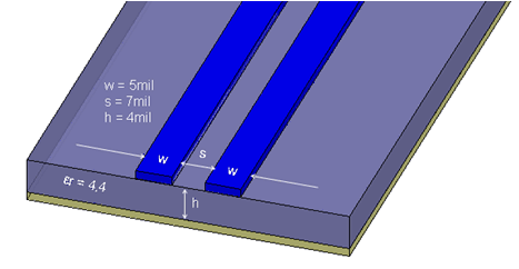 Figure 10-1 Differential Microstrip PCB Trace Geometry Example
To avoid impedance discontinuities the high-speed serial signals should be routed on a PCB on either the top or bottom PCB layers in microstrip format with no vias. If vias are unavoidable, an absolute minimum number of vias need to be used. The vias should be made to stretch through the entire PCB thickness (as shown in Figure 10-2) to connect microstrip traces on the top and bottom layers of the PCB so as to leave no via stubs that can severely impact the performance. If stripline traces are absolutely necessary, and if via back-drilling is not possible, then the routing layers should be chosen so as to have via stubs that are shorter than 10 mils.
All unused internal layer via pads on high-speed signal vias should be removed to further improve impedance matching. On the high-speed side, the HSRXAP/HSRXAN signals are more sensitive to impedance discontinuities introduced by vias than HSTXAP/HSTXAN signals. For that reason, if only some of those signals need to be routed with vias, then the latter should be routed with vias and the former with no vias.
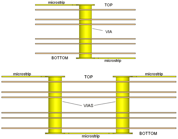 Figure 10-2 Examples of High-speed PCB Traces With Vias That Have no Via Stubs and no Via Pads on Internal Layers
To further improve on impedance matching, differential vias with neighboring ground vias can be used as shown in Figure 10-3. The optimum dimensions of such a differential via structure depend on various parameters such as the trace geometry, dielectric material, as well as the PCB layer stack-up. A 3D electromagnetic field solver can be used to find the optimum via dimensions.
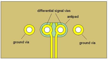 Figure 10-3 A Differential PCB Via Structure (Top View)
PCB traces connected to the HSRXAP/HSRXAN pins should have differential insertion loss of less than 25 dB at 5 GHz.
Surface-mount connector pads such as those used with the SFP/SFP+ module connectors are wider and hence have characteristic impedance that is lower than the regular high-speed PCB traces. If the pads are more than 2 times wider than the PCB traces, the pads’ impedance needs to be increased to minimize impedance discontinuities. The easy way of increasing the pads’ impedance is to cut out the reference plane immediately under those pads as shown in Figure 10-4 so as to have the pads refer to a reference plane on lower layers while maintaining 100 Ω differential characteristic impedance.
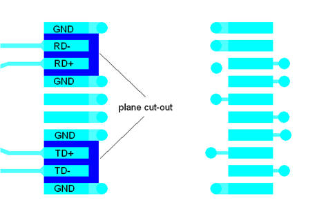 Figure 10-4 Surface-mount Connector Pads
10.1.1.2 AC-coupling
A 0.1-uF series AC-coupling capacitor should be connected to each of the high-speed data path pins INA[3:0]P/INA[3:0]N, HSRXAP/HSRXAN, OUTA[3:0]P/OUTA[3:0]N, and HSTXAP/HSTXAN. If the TLK10031 high-speed side data path pins are connected to SFP/SFP+ optical modules with internal AC-coupling capacitors, then no external capacitors should be used. Adding additional series capacitors may severely impact the performance.
To avoid impedance discontinuities, it is strongly recommended where possible to make the transmission line trace width closely match the AC-coupling capacitor pad size. Smaller capacitor packages such as 0201 make it easy to meet that condition.
10.1.2 TLK10031 Clocks: REFCLK, CLKOUT
10.1.2.1 General Information
The TLK10031 device requires a low-jitter reference clock to work. The reference clock can be provided on the REFCLK0P/N or REFCLK1P/N pins. Both reference clock input pins have internal 100-Ω differential terminations, so they do not need any external terminations. Both reference clock inputs must be AC-coupled with preferably 0.1-µF capacitors. The two channels (A and B) can have same or different reference clocks.
The TLK10031 serial receiver recovers clock and data from the incoming serial data. The recovered byte clock is made available on the CLKOUTAP/N pins. The CLKOUTAP/N CML output pins must be AC-coupled with 0.1-µF AC-coupling capacitors.
10.1.2.2 External Clock Connections
An external clock jitter cleaner, such as Texas Instruments CDCE72010 or CDCM7005, may be used when needed to provide a low jitter reference clock. An example external clock jitter cleaner connection for channel A is shown in Figure 10-5.
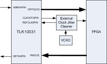 Figure 10-5 An External Clock Jitter Cleaner Connection Example for Channel A
10.1.2.3 TLK10031 Control Pins and Interfaces
The TLK10031 device features a number of control pins and interfaces, some of which are described as follows.
10.1.2.3.1 MDIO Interface
The TLK10031 supports the Management Data Input/Output (MDIO) Interface as defined in Clause 22 of the IEEE 802.3 Ethernet specification. The MDIO allows register-based management and control of the serial links.
The MDIO Management Interface consists of a bi-directional data path (MDIO) and a clock reference (MDC). The port address is determined by the PRTAD[4:0] control pins.
The MDIO pin requires a pullup to VDDO[1:0]. No pullup is needed on the MDC pin if driven with a push-pull MDIO master, but a pullup to VDDO[1:0] is needed if driven with an open-drain MDIO master.
10.1.2.3.2 JTAG Interface
The JTAG interface is mostly used for device test. The JTAG interface operates through the TDI, TDO, TMS, TCK, and TRST_N pins. If not used, all the pins can be left unconnected except TDI and TCK which must be grounded.
10.1.2.3.3 Unused Pins
As a general guideline, any unused LVCMOS input pin needs to be grounded and any unused LVCMOS output pin can be left unconnected. Unused CML differential output pins can be left unconnected. Unused CML differential input pins should be tied to ground through a shared 100-Ω resistor.
10.2 Layout Example
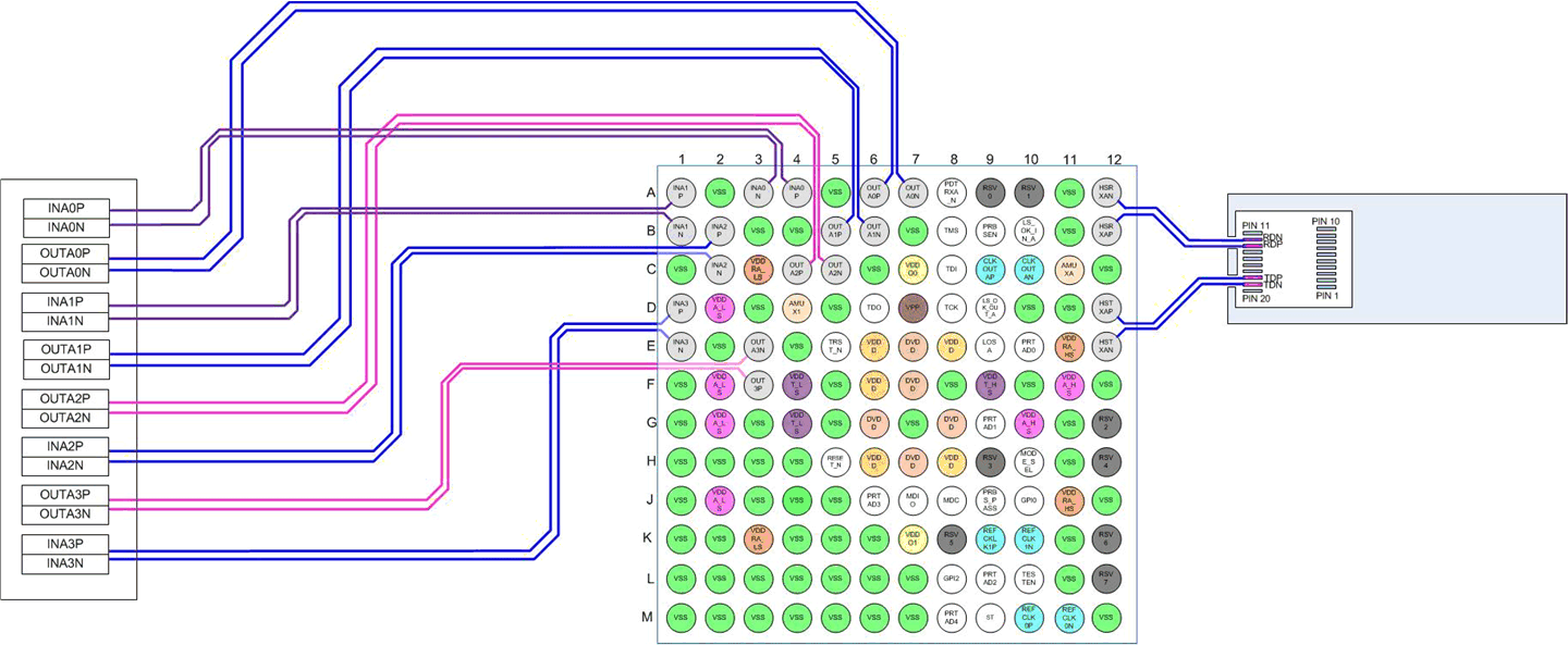 Figure 10-6 Pinout and Routing