ZHCSC51 March 2014 TLC5955
PRODUCTION DATA.
- 1 特性
- 2 应用范围
- 3 说明
- 4 修订历史记录
- 5 Terminal Configurations and Functions
- 6 Specifications
- 7 Parameter Measurement Information
-
8 Detailed Description
- 8.1 Overview
- 8.2 Functional Block Diagram
- 8.3 Feature Description
- 8.4 Device Functional Modes
- 9 Applications and Implementation
- 10Power Supply Recommendations
- 11Layout
- 12器件和文档支持
- 13机械封装和可订购信息
封装选项
机械数据 (封装 | 引脚)
散热焊盘机械数据 (封装 | 引脚)
订购信息
5 Terminal Configurations and Functions
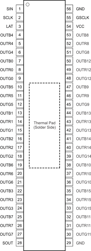
DCA Package
HTSSOP-56
(Top View)
RTQ Package
QFN-56
(Top View)
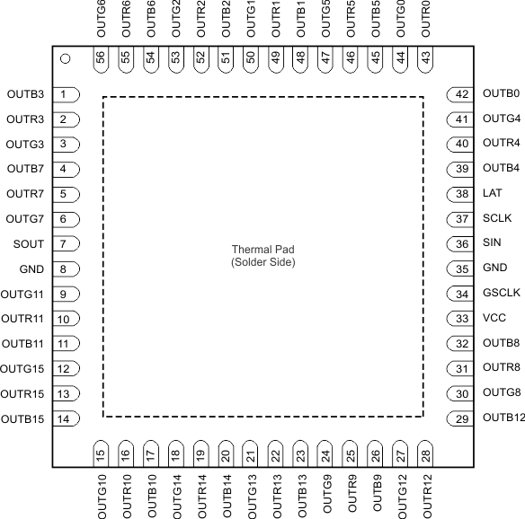
Terminal Functions
| TERMINAL | I/O | DESCRIPTION | ||
|---|---|---|---|---|
| NAME | DCA NUMBER | RTQ NUMBER | ||
| GND | 29, 56 | 8, 35 | — | Power ground |
| GSCLK | 55 | 34 | I | Reference clock for the grayscale (GS) pulse width modulation (PWM) control for all outputs. Each GSCLK rising edge increments the grayscale counter for PWM control. When the LAT signal is input for a GS data write with the timing reset mode enabled, all constant-current outputs (OUTX0-OUTX15, where X = R, G, or B) are forced off, the grayscale counter is reset to 0, and the grayscale PWM timing controller is initialized. |
| LAT | 3 | 38 | I | The LAT rising edge either latches the data from the common shift register into the GS data latch when the MSB of the common shift register is 0 or latches the data into the control data latch when the MSB of the common shift register is 1. When the display timing reset bit (TMGRST) in the control data latch is 1, the grayscale counter initialized at the LAT signal is input for a grayscale data write. Dot correction (DC) data in the control data latch are copied to DC data latch at the same time. |
| OUTB0 to OUTB15 | 4, 7, 10, 13, 16, 19, 22, 25, 32, 35, 38, 41, 44, 47, 50, 53 | 1, 4, 11, 14, 17, 20, 23, 26, 29, 32, 39, 42, 45, 48, 51, 54 | O | Constant-current outputs for the blue color group. Multiple outputs can be configured in parallel to increase the constant-current capability. Different voltages can be applied to each output. |
| OUTG0 to OUTG15 | 6, 9, 12, 15, 18, 21, 24, 27, 30, 33, 36, 39, 42, 45, 48, 51 | 3, 6, 9, 12, 15, 18, 21, 24, 27, 30, 41, 44, 47, 50, 53, 56 | O | Constant-current outputs for the green color group. Multiple outputs can be configured in parallel to increase the constant-current capability. Different voltages can be applied to each output. |
| OUTR0 to OUTR15 | 5, 8, 11, 14, 17, 20, 23, 26, 31, 34, 37, 40, 43, 46, 49, 52 | 2, 5, 10, 13, 16, 19, 22, 25, 28, 31, 40, 43, 46, 49, 52, 55 | O | Constant-current outputs for the red color group. Multiple outputs can be configured in parallel to increase the constant-current capability. Different voltages can be applied to each output. |
| SCLK | 2 | 37 | I | Serial data shift clock. Data present on SIN are shifted to the LSB of the common shift register with the SCLK rising edge. Data in the shift register are shifted toward the MSB at each SCLK rising edge. The MSB data of the common shift register appears on SOUT. |
| SIN | 1 | 36 | I | Serial data input for the 769-bit common shift register. |
| SOUT | 28 | 7 | O | This bit is the serial data output of the 769-bit common shift register. LED open detection (LOD) and LED short detection (LSD) can be read out with SOUT in the form of status information data (SID) after the LAT falling edge is input for a GS data write. SOUT is connected to the MSB of the 769-bit common shift register. Data are clocked out at the SCLK rising edge. |
| VCC | 54 | 33 | — | Power-supply voltage |
| Thermal pad | — | The thermal pad is not connected to GND internally. The thermal pad must be connected to GND via the PCB. |
||