ZHCSC51 March   2014 TLC5955

PRODUCTION DATA.  

  1. 特性
  2. 应用范围
  3. 说明
  4. 修订历史记录
  5. Terminal Configurations and Functions
  6. Specifications
    1. 6.1 Absolute Maximum Ratings
    2. 6.2 Handling Ratings
    3. 6.3 Recommended Operating Conditions
    4. 6.4 Thermal Information
    5. 6.5 Electrical Characteristics
    6. 6.6 Switching Characteristics
    7. 6.7 Typical Characteristics
  7. Parameter Measurement Information
    1. 7.1 Terminal-Equivalent Input and Output Schematic Diagrams
    2. 7.2 Test Circuits
    3. 7.3 Timing Diagrams
  8. Detailed Description
    1. 8.1 Overview
    2. 8.2 Functional Block Diagram
    3. 8.3 Feature Description
      1. 8.3.1 Output Current Calculation
      2. 8.3.2 Register and Data Latch Configuration
        1. 8.3.2.1 769-Bit Common Shift Register
        2. 8.3.2.2 Grayscale (GS) Data Latch
        3. 8.3.2.3 Control Data Latch
        4. 8.3.2.4 Dot Correction (DC) Data Latch
        5. 8.3.2.5 Maximum Current (MC) Data Latch
        6. 8.3.2.6 Global Brightness Control (BC) Data Latch
        7. 8.3.2.7 Function Control (FC) Data Latch
      3. 8.3.3 Status Information Data (SID)
      4. 8.3.4 LED Open Detection (LOD)
      5. 8.3.5 LED Short Detection (LSD)
      6. 8.3.6 Noise Reduction
    4. 8.4 Device Functional Modes
      1. 8.4.1 Maximum Current Control (MC) Function
      2. 8.4.2 Dot Correction (DC) Function
      3. 8.4.3 Global Brightness Control (BC) Function
      4. 8.4.4 Grayscale (GS) Function (PWM Control)
        1. 8.4.4.1 Conventional PWM Control
        2. 8.4.4.2 Enhanced Spectrum (ES) PWM Control
        3. 8.4.4.3 Auto Display Repeat Function
        4. 8.4.4.4 Display Timing Reset Function
        5. 8.4.4.5 Auto Data Refresh Function
  9. Applications and Implementation
    1. 9.1 Application Information
    2. 9.2 Typical Application
      1. 9.2.1 Daisy-Chain Application
        1. 9.2.1.1 Design Requirements
        2. 9.2.1.2 Detailed Design Procedure
          1. 9.2.1.2.1 Step-by-Step Design Procedure
          2. 9.2.1.2.2 Maximum Current (MC) Data
          3. 9.2.1.2.3 Global Brightness Control (BC) Data
          4. 9.2.1.2.4 Dot Correction (DC) Data
          5. 9.2.1.2.5 Grayscale (GS) Data
          6. 9.2.1.2.6 Other Control Data
        3. 9.2.1.3 Application Curves
  10. 10Power Supply Recommendations
  11. 11Layout
    1. 11.1 Layout Guidelines
    2. 11.2 Layout Example
  12. 12器件和文档支持
    1. 12.1 器件支持
      1. 12.1.1 开发支持
    2. 12.2 文档支持
      1. 12.2.1 相关文档 
    3. 12.3 Trademarks
    4. 12.4 Electrostatic Discharge Caution
    5. 12.5 Glossary
  13. 13机械封装和可订购信息

封装选项

机械数据 (封装 | 引脚)
散热焊盘机械数据 (封装 | 引脚)
订购信息

11 Layout

11.1 Layout Guidelines

  1. Place the decoupling capacitor near the VCC and GND terminals.
  2. Route the GND pattern as widely as possible for large GND currents. Maximum GND current is approximately 1.53 A.
  3. Routing between the LED cathode side and the device OUTXn should be as short and straight as possible to reduce wire inductance.
  4. The PowerPAD must be connected to the GND layer because the pad is not internally connected to GND and should be connected to a heat sink layer to reduce device temperature.

11.2 Layout Example

ai_layout_bvs237.gif
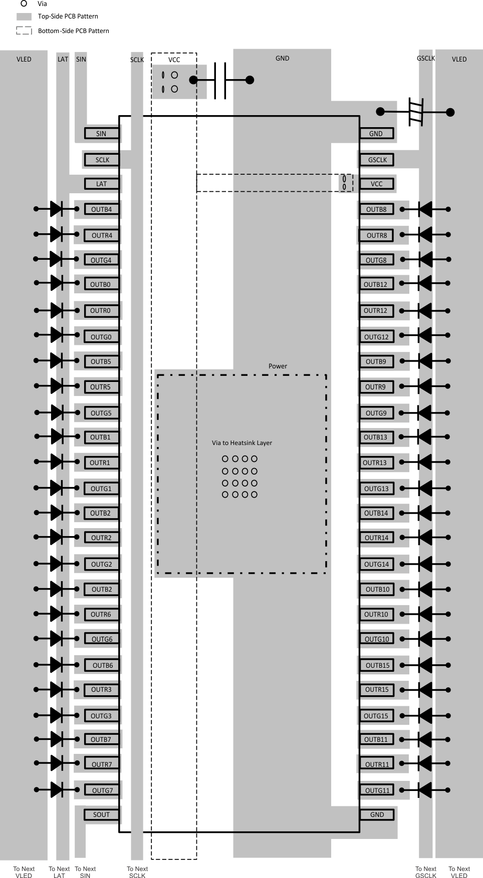
Figure 36. Layout Example