SLLS228G December 1995 – August 2015 TIR1000
UNLESS OTHERWISE NOTED, this document contains PRODUCTION DATA.
- 1 Features
- 2 Applications
- 3 Description
- 4 Revision History
- 5 Pin Configuration and Functions
- 6 Specifications
- 7 Detailed Description
- 8 Application and Implementation
- 9 Power Supply Recommendations
- 10Layout
- 11Device and Documentation Support
- 12Mechanical, Packaging, and Orderable Information
封装选项
机械数据 (封装 | 引脚)
散热焊盘机械数据 (封装 | 引脚)
- PS|8
订购信息
10 Layout
10.1 Layout Guidelines
There is no fundamental information about how many layers should be used and how the board stackup should look. Again, the easiest way the get good results is to use the design from the EVMs of Texas Instruments. The magazine Elektronik Praxis
(1) Elektronik-Praxis: Die Leiterplatte 2010, Ausgabe 11/06, P72-77
has published an article with an analysis of different board stackups. These are listed in Table 3. Generally, the use of microstrip traces needs at least two layers, whereas one of them must be a GND plane. Better is the use of a four-layer PCB, with a GND and a VCC plane and two signal layers. If the circuit is complex and signals must be routed as stripline, because of propagation delay and/or characteristic impedance, a six-layer stackup should be used.
Table 3. Possible Board Stackup on a Four-Layer PCB
| MODEL 1 | MODEL 2 | MODEL 3 | MODEL 4 | |
|---|---|---|---|---|
| Layer 1 | SIG | SIG | SIG | GND |
| Layer 2 | SIG | GND | GND | SIG |
| Layer 3 | VCC | VCC | SIG | VCC |
| Layer 4 | GND | SIG | VCC | SIG |
| Decoupling | Good | Good | Bad | Bad |
| EMC | Bad | Bad | Bad | Bad |
| Signal integrity | Bad | Bad | Good | Bad |
| Self disturbance | Satisfaction | Satisfaction | Satisfaction | High |
Avoid right-angle bends in a trace and try to route them at least with two 45° corners. To minimize any impedance change, the best routing would be a round bend as shown in Figure 13.
 Figure 13. Poor and Good Right Angle Bends
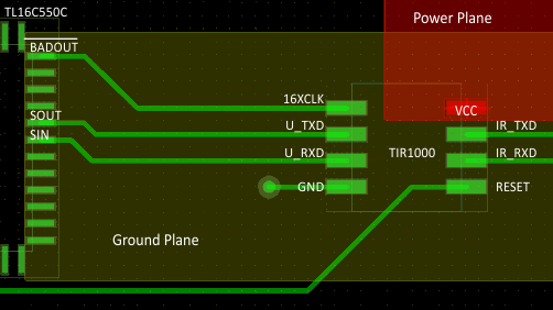
10.2 Layout Example
 Figure 14. Layout Example