SLES032E June 2002 – September 2014 THS8200
PRODUCTION DATA.
- 1 Device Overview
- 2 Revision History
- 3 Terminal Configuration and Functions
-
4 Specifications
- 4.1 Absolute Maximum Ratings
- 4.2 Handling Ratings
- 4.3 Recommended Operating Conditions
- 4.4 Power Consumption Summary
- 4.5 Power Supply
- 4.6 Digital Inputs, DC Characteristics
- 4.7 Analog (DAC) Outputs
- 4.8 Nonlinearity
- 4.9 Analog Output Bandwidth (sinx/x corrected) at fS = 205 MSPS
- 4.10 Output Compliance vs Full-Scale Adjustment Resistor Value
- 4.11 Vertical Sync of the HDTV 1080I Format Preset in First and Second Field, and Horizontal Line Waveform Detail
-
5 Functional Overview
- 5.1
Data Manager (DMAN)
- 5.1.1 Interpolating Finite Impulse Responses Filter (IFIR)
- 5.1.2 Color-Space Conversion (CSC)
- 5.1.3 Clip/Shift/Multiplier (CSM)
- 5.1.4 Digital Multiplexer (DIGMUX)
- 5.1.5 Display Timing Generator (DTG)
- 5.1.6 Clock Generator (CGEN)
- 5.1.7 Clock Driver (CDRV)
- 5.1.8 I2C Host Interface (I2CSLAVE)
- 5.1.9 Test Block (TST)
- 5.1.10 D/A Converters (DACs)
- 5.1
Data Manager (DMAN)
-
6 Detailed Functional Description
- 6.1 Data Manager (DMAN)
- 6.2 Input Interface Formats
- 6.3 Clock Generator (CGEN)/Clock Driver (CDRV)
- 6.4 Color Space Conversion (CSC)
- 6.5 Clip/Shift/Multiplier (CSM)
- 6.6 Interpolating Finite Impulse Response Filter (IFIR)
- 6.7
Display Timing Generator (DTG)
- 6.7.1 Overview of Functionality
- 6.7.2 Functional Description
- 6.7.3
DTG Line Type Overview
- 6.7.3.1 HDTV Mode
- 6.7.3.2 Active Video
- 6.7.3.3 FULL NTSP (Full Normal Tri-Level Sync Pulse)
- 6.7.3.4 NTSP NTSP (Normal Tri-Level Sync Pulse/Normal Tri-Level Sync Pulse)
- 6.7.3.5 BTSP BTSP (Broad Pulse and Tri-Level Sync Pulse/Broad Pulse and Tri-Level Sync Pulse)
- 6.7.3.6 NTSP BTSP (Normal Tri-Level Sync Pulse/ Broad Pulse and Tri-Level Sync Pulse)
- 6.7.3.7 BTSP NTSP (Broad Pulse and Tri-Level Sync Pulse/Normal Tri-Level Sync Pulse)
- 6.7.3.8 Full BTSP (Full Broad Pulse and Tri-Level Sync Pulse)
- 6.7.3.9 SDTV Mode
- 6.7.3.10 NEQ_NEQ (Negative Equalization Pulse/Negative Equalization Pulse)
- 6.7.3.11 FULL_BSP (Full Broad Sync Pulse)
- 6.7.3.12 BSP_BSP (Broad Sync Pulse/Broad Sync Pulse)
- 6.7.3.13 FULL_NSP (Full Normal Sync Pulse)
- 6.7.3.14 NEQ_BSP (Negative Equalization Pulse/Broad Sync Pulse)
- 6.7.3.15 BSP_NEQ (Broad Sync Pulse/Negative Equalization Pulse)
- 6.7.3.16 FULL_NEQ (Full Negative Equalization Pulse)
- 6.7.3.17 NSP_ACTIVE (Normal Sync Pulse/Active Video)
- 6.7.3.18 ACTIVE_NEQ (Active Video/Negative Equalization Pulse)
- 6.7.3.19 ACTIVE VIDEO
- 6.8
D/A Conversion
- 6.8.1 RGB Output Without Sync Signal Insertion/General-Purpose Application DAC
- 6.8.2 SMPTE-Compatible RGB Output With Sync Signal Inserted on G (Green) Channel
- 6.8.3 SMPTE-Compatible Analog-Level Output With Sync Inserted on All RGB Channels
- 6.8.4 SMPTE-Compatible YPbPr Output With Sync Signal Inserted on Y Channel Only
- 6.8.5 SMPTE-Compatible YPbPr Output With Sync Signal Inserted on All Channels
- 6.8.6 Summary of Supported Video Formats
- 6.9 Test Functions
- 6.10 Power Down
- 6.11 CGMS Insertion
- 6.12 I2C Interface
-
7 I2C Registers
- 7.1 I2C Register Map
- 7.2
Register Descriptions
- 7.2.1 System Control (Sub-Addresses 0x02−0x03)
- 7.2.2 Color Space Conversion Control (Sub-Addresses 0x04−0x19)
- 7.2.3 Test Control (Sub-Addresses 0x1A−0x1B)
- 7.2.4 Data Path Control (Sub-Address 0x1C)
- 7.2.5 Display Timing Generator Control, Part 1 (Sub-Addresses 0x1D−0x3C)
- 7.2.6 DAC Control (Sub-Addresses 0x3D−0x40)
- 7.2.7 Clip/Shift/Multiplier Control (Sub-Addresses 0x41−0x4F)
- 7.2.8 Display Timing Generator Control, Part 2 (Sub-Addresses 0x50−0x82)
- 7.2.9 CGMS Control (Sub-Addresses 0x83−0x85)
- 7.3 THS8200 Preset Mode Line Type Definitions
- 8 Application Information
- 9 Device and Documentation Support
- 10Mechanical, Packaging, and Orderable Information
3 Terminal Configuration and Functions
Figure 3-1 shows the pinout for the PFP package.
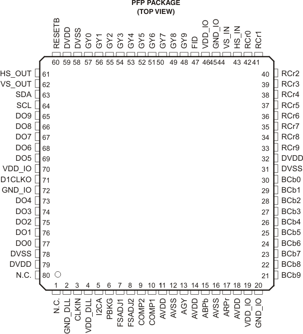 Figure 3-1 80-Pin PFP Package (Top View)
3.1 Terminal Functions
Table 3-1 describes the signals for the device.
Table 3-1 Terminal Functions
| TERMINAL | I/O (1) | DESCRIPTION | |
|---|---|---|---|
| NAME | NO. | ||
| ABPb | 15 | O | Analog output of DAC2. See AGY. |
| ARPr | 17 | O | Analog output of DAC3. See AGY. |
| AGY | 13 | O | Analog output of DAC1. With the proper setting of FSADJ<n>, this output is capable of driving 1.3-V full scale into a 37.5-Ω load. |
| AVDD | 11, 14, 18 | PWR | Analog power supply, nominal 3.3 V |
| AVSS | 12, 16 | PWR | Analog ground |
| BCb[9:0] | 21 - 30 | I | 10-bit video data input port. All 10 bits or the 8 MSB of this port can be connected to the video data source. In 30-bit mode, the B data of RGB, or the Cb data of YCbCr, should be connected to this port. In 10-bit input mode, this port is unused. In 20-bit input mode, this port is used for CbCr input data. |
| CLKIN | 3 | I | Main clock input. Video input data on the GY[9:0]/BCb[9:0]/RCr[9:0] ports should be synchronized to CLKIN. Depending on the input data format, CLKIN is supplied to THS8200 at 1x or 2x the pixel clock frequency. |
| COMP1 | 10 | P | Compensation pin for the internal reference amplifier. A 0.1-µF capacitor should be connected between COMP1 and analog power supply AVDD. |
| COMP2 | 9 | P | Compensation pin for the internal reference amplifier. A 0.1-µF capacitor should be connected between COMP2 and analog power supply AVDD. |
| D1CLKO | 71 | O | Video ITU-R.BT656-compliant clock output. This clock output is off by default and should be activated by an I2C register setting. |
| DO[9:5] DO[4:0] |
65-69 73-77 |
O | ITU-R.BT656 compliant video data output port. Only available when ITU-R.BT656 input format is used. Can be used to connect to external PAL/NTSC video encoder. This port is off by default and should be activated by an I2C register setting. |
| DVDD | 32, 59, 79 | PWR | Digital core power, nominal 1.8 V |
| DVSS | 31, 58, 78 | PWR | Digital core ground |
| FID | 47 | I | Field identification signal for interlaced video formats. In slave timing mode, this is an input from the video data source. In master timing mode this signal is unused, as only progressive-scan VESA formats are supported in master mode. |
| FSADJ1 | 7 | P | Full scale adjustment control 1. A resistor should be connected between FSADJ1 and analog ground AGND to control the full-scale output current of the DAC output channels. The data_fsadj I2C programming register can be used to select between two full-scale ranges, determined by FSADJ1 or FSADJ2. For 700-mV video output (1 Vpp including sync), the nominal value is 2.99 kΩ ; for 1.0-Vpp video output (1.3 Vpp including sync) output the nominal value is 2.08 kΩ. |
| FSADJ2 | 8 | P | Full scale adjustment control 2. See FSADJ1. |
| GND_DLL | 2 | PWR | Ground of clock doubler. Should be connected to analog ground. |
| GND_IO | 20, 45, 72 | PWR | I/O ring ground |
| GY[9:0] | 48-57 | I | 10-bit video data input port. All 10 bits or the 8 MSB of this port can be connected to the video data source. The G data of RGB or the Y data of YCbCr should be connected to this port. Port used in 10-bit mode for CbYCrY video input data; in 20-bit input mode for Y data. |
| HS_IN | 43 | I/O | Horizontal source synchronization. In slave timing mode, this is an input from the video data source. In master timing mode, this is an output to the video data source with programmable timing and polarity, serving as a horizontal data qualification signal to the video source. |
| HS_OUT | 61 | O | Horizontal sync output (to display). Irrespective of slave/master timing mode configuration, this is always an output with timing generated by the DTG. |
| I2CA | 5 | I | I2C device address LSB selection |
| N.C. | 1, 80 | I | Manufacturing test input. Must be tied to GND for normal operation. |
| PBKG (VSS) | 6 | PWR | Substrate ground. Should be connected to analog ground. |
| RCr[9:0] | 33-42 | I | 10-bit video data input port. All 10-bits or the 8 MSB of this port can be connected to the video data source. In 30-bit mode, the R data of RGB or the Cr data of YCbCr should be connected to this port. In the 10- /20-bit input mode, this port is unused. For some input formats this port is unused. |
| RESETB | 60 | I | Software reset pin (active low). The minimum reset duration is 200 ns. |
| SCL | 64 | B | Serial clock line of I2C bus interface. Open-collector. Maximum specified clock speed is 400 kHz (fast I2C). |
| SDA | 63 | B | Serial data line of I2C bus interface. Open-collector. |
| VDD_DLL | 4 | PWR | Power supply of clock doubler, 1.8 V nominal |
| VDD_IO | 19, 46, 70 | PWR | I/O ring power, 1.8 V or 3.3 V nominal |
| VS_IN | 44 | I/O | Vertical source synchronization. In slave timing mode, this is an input from the video data source. In master timing mode, this is an output to the video data source with programmable timing and polarity, serving as a vertical data qualification signal to the video source. |
| VS_OUT | 62 | O | Vertical sync output (to display). Regardless of slave/master timing mode configuration, this is always an output with timing generated by the DTG. |
(1) I = input, O = output, B = bidirectional, PWR = power or ground, P = passive