SLES032E June 2002 – September 2014 THS8200
PRODUCTION DATA.
- 1 Device Overview
- 2 Revision History
- 3 Terminal Configuration and Functions
-
4 Specifications
- 4.1 Absolute Maximum Ratings
- 4.2 Handling Ratings
- 4.3 Recommended Operating Conditions
- 4.4 Power Consumption Summary
- 4.5 Power Supply
- 4.6 Digital Inputs, DC Characteristics
- 4.7 Analog (DAC) Outputs
- 4.8 Nonlinearity
- 4.9 Analog Output Bandwidth (sinx/x corrected) at fS = 205 MSPS
- 4.10 Output Compliance vs Full-Scale Adjustment Resistor Value
- 4.11 Vertical Sync of the HDTV 1080I Format Preset in First and Second Field, and Horizontal Line Waveform Detail
-
5 Functional Overview
- 5.1
Data Manager (DMAN)
- 5.1.1 Interpolating Finite Impulse Responses Filter (IFIR)
- 5.1.2 Color-Space Conversion (CSC)
- 5.1.3 Clip/Shift/Multiplier (CSM)
- 5.1.4 Digital Multiplexer (DIGMUX)
- 5.1.5 Display Timing Generator (DTG)
- 5.1.6 Clock Generator (CGEN)
- 5.1.7 Clock Driver (CDRV)
- 5.1.8 I2C Host Interface (I2CSLAVE)
- 5.1.9 Test Block (TST)
- 5.1.10 D/A Converters (DACs)
- 5.1
Data Manager (DMAN)
-
6 Detailed Functional Description
- 6.1 Data Manager (DMAN)
- 6.2 Input Interface Formats
- 6.3 Clock Generator (CGEN)/Clock Driver (CDRV)
- 6.4 Color Space Conversion (CSC)
- 6.5 Clip/Shift/Multiplier (CSM)
- 6.6 Interpolating Finite Impulse Response Filter (IFIR)
- 6.7
Display Timing Generator (DTG)
- 6.7.1 Overview of Functionality
- 6.7.2 Functional Description
- 6.7.3
DTG Line Type Overview
- 6.7.3.1 HDTV Mode
- 6.7.3.2 Active Video
- 6.7.3.3 FULL NTSP (Full Normal Tri-Level Sync Pulse)
- 6.7.3.4 NTSP NTSP (Normal Tri-Level Sync Pulse/Normal Tri-Level Sync Pulse)
- 6.7.3.5 BTSP BTSP (Broad Pulse and Tri-Level Sync Pulse/Broad Pulse and Tri-Level Sync Pulse)
- 6.7.3.6 NTSP BTSP (Normal Tri-Level Sync Pulse/ Broad Pulse and Tri-Level Sync Pulse)
- 6.7.3.7 BTSP NTSP (Broad Pulse and Tri-Level Sync Pulse/Normal Tri-Level Sync Pulse)
- 6.7.3.8 Full BTSP (Full Broad Pulse and Tri-Level Sync Pulse)
- 6.7.3.9 SDTV Mode
- 6.7.3.10 NEQ_NEQ (Negative Equalization Pulse/Negative Equalization Pulse)
- 6.7.3.11 FULL_BSP (Full Broad Sync Pulse)
- 6.7.3.12 BSP_BSP (Broad Sync Pulse/Broad Sync Pulse)
- 6.7.3.13 FULL_NSP (Full Normal Sync Pulse)
- 6.7.3.14 NEQ_BSP (Negative Equalization Pulse/Broad Sync Pulse)
- 6.7.3.15 BSP_NEQ (Broad Sync Pulse/Negative Equalization Pulse)
- 6.7.3.16 FULL_NEQ (Full Negative Equalization Pulse)
- 6.7.3.17 NSP_ACTIVE (Normal Sync Pulse/Active Video)
- 6.7.3.18 ACTIVE_NEQ (Active Video/Negative Equalization Pulse)
- 6.7.3.19 ACTIVE VIDEO
- 6.8
D/A Conversion
- 6.8.1 RGB Output Without Sync Signal Insertion/General-Purpose Application DAC
- 6.8.2 SMPTE-Compatible RGB Output With Sync Signal Inserted on G (Green) Channel
- 6.8.3 SMPTE-Compatible Analog-Level Output With Sync Inserted on All RGB Channels
- 6.8.4 SMPTE-Compatible YPbPr Output With Sync Signal Inserted on Y Channel Only
- 6.8.5 SMPTE-Compatible YPbPr Output With Sync Signal Inserted on All Channels
- 6.8.6 Summary of Supported Video Formats
- 6.9 Test Functions
- 6.10 Power Down
- 6.11 CGMS Insertion
- 6.12 I2C Interface
-
7 I2C Registers
- 7.1 I2C Register Map
- 7.2
Register Descriptions
- 7.2.1 System Control (Sub-Addresses 0x02−0x03)
- 7.2.2 Color Space Conversion Control (Sub-Addresses 0x04−0x19)
- 7.2.3 Test Control (Sub-Addresses 0x1A−0x1B)
- 7.2.4 Data Path Control (Sub-Address 0x1C)
- 7.2.5 Display Timing Generator Control, Part 1 (Sub-Addresses 0x1D−0x3C)
- 7.2.6 DAC Control (Sub-Addresses 0x3D−0x40)
- 7.2.7 Clip/Shift/Multiplier Control (Sub-Addresses 0x41−0x4F)
- 7.2.8 Display Timing Generator Control, Part 2 (Sub-Addresses 0x50−0x82)
- 7.2.9 CGMS Control (Sub-Addresses 0x83−0x85)
- 7.3 THS8200 Preset Mode Line Type Definitions
- 8 Application Information
- 9 Device and Documentation Support
- 10Mechanical, Packaging, and Orderable Information
6 Detailed Functional Description
6.1 Data Manager (DMAN)
Table 6-1 Supported Input Formats
| INPUT INTERFACE | TIMING CONTROL | SYNCHRONIZATION | |||||||
|---|---|---|---|---|---|---|---|---|---|
| 30 BIT | 20 BIT | 10 BIT (1) | 16 BIT | 15 BIT | EMBEDDED TIMING | DEDICATED TIMING | MASTER | SLAVE | |
| [PRESET] HDTV-SMPTE296M progressive (720P) |
X (4:4:4) | X (4:2:2) | X | X | X | ||||
| [PRESET] HDTV-SMPTE274M progressive (1080P) |
X (4:4:4) | X (4:2:2) | X | X | X | ||||
| [PRESET] HDTV-SMPTE274M progressive (1080I) |
X (4:4:4) | X (4:2:2) | X | X | |||||
| [GENERIC] HDTV | X (4:4:4) | X (4:2:2) | X | X | X | ||||
| [PRESET] SDTV-ITU.1358 (525P) |
X (4:4:4) | X (4:2:2) | X (2) | X | X (5) | X | |||
| [PRESET] SDTV-ITU-R.BT470 (525I) |
X (4:4:4) | X (4:2:2) | X (3) | X | X (5) | X | |||
| [PRESET] SDTV-ITU-R.BT470 (625i) |
X (4:4:4) | X (4:2:2) | X (3) | X | X (5) | X | |||
| [GENERIC] SDTV | X (4:4:4) | X (4:2:2) | X | X | X | ||||
| [PRESET] VESA | X (4) | X (4) | X (4) | X | X | X | |||
Table 6-1 summarizes all supported video mode configurations.
Each video mode is characterized by three attributes:
- Input Interface: Data is accepted over 10-, 20- or 30-bit interface (or 8- ,16-, 24-bit interface for 8-bit data when using 8 MSBs of each input data bus and connecting 2 LSBs to ground). This selection is controlled by the dman_cntl register.
- Timing control: Video timing is either embedded in the data stream or supplied by dedicated timing signals. In the latter case additional Hsync (HS_IN), Vsync (VS_IN) and FieldID (FID) input signals are required to synchronize the video data source and THS8200 in the case of slave timing mode. This selection is controlled by the dtg2_embedded_timing register.
- Synchronization: Video timing either is supplied to the device (slave) or the THS8200 requests video data from the source (master). This selection is controlled by the chip_ms register.
NOTE
Device operation with combinations of settings for the dman_cntl, dtg2_embedded_timing and chip_ms registers that result in operating modes not marked in Table 6-1 is not assured. See detailed register map description for actual register settings.
Furthermore, Table 6-1 shows for which modes presets are defined. When in a preset video mode, the line-type/breakpoint-pairs that define the frame format (see Section 6.7) are preprogrammed. Therefore the user does not need to define the table with line type/breakpoint settings, nor does the field and frame size need to be programmed. However, when in preset mode, the horizontal parameters (all dtg1_spec_x registers for the line types used by the preset setting, and dtg1_total_pixels registers) still need to be programmed. Presets are available for most popular DTV video formats. Alternatively, generic modes for SDTV, HDTV or VESA can be selected, which allow full programmability of the field/frame sizes and DTG parameters.
Note from the table that:
- If embedded timing is used, the device is always in slave mode, because the data stream supplied to THS8200 contains the video timing information.
- Master operation is only supported for PC graphics (VESA) formats.
- In HDTV modes with embedded timing, data is supplied to the device over a 20-bit interface, as defined in SMPTE274/296M.
- In SDTV modes with embedded timing, data is supplied to the device over a 10-bit interface. When the video format is interlaced, this interface is known as ITU-R.BT656 (525I, 625I). When the video format is progressive, only 525P is supported with embedded timing. The 625P interface can be supported with dedicated timing, using the SDTV generic mode.
- In generic modes with dedicated timing, both 20 bits (4:2:2) and 30 bits (4:4:4) are supported.
- In PC graphics modes (VESA generic), input data is either over the 30-bit interface or over the 16-/15-bit interface and always has dedicated timing. Note that the 16-bit interface is not equivalent to a 2x8-bit version of the 20-bit interface; see Section 6.2 for details.
6.2 Input Interface Formats
The following figures define the input video format for each input mode, as selected by the data_dman_cntl register setting. Video data is always clocked in at the rising edge of CLKIN.
NOTE
For 8-bit operation with 10-bit input buses, connect only the 8 MSBs of each input bus used, and tie the 2 LSBs to ground.
- 30-bit YCbCr/RGB 4:4:4
- 20-bit YCbCr 4:2:2
- 10-bit YCbCr 4:2:2 (ITU mode)
- 16-bit RGB 4:4:4
- 15-bit RGB 4:4:4
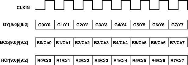 Figure 6-1 24-/30-Bit RGB or YCbCr Data Format
CLKIN is equal to the 1x pixel clock. The pixel clock equals the rate of the Y input and is 2x the rate of the 2 other channels in this input format where Cb and Cr are multiplexed onto the same input bus.
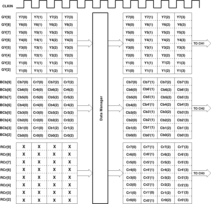 Figure 6-2 20-/16-Bit YCbCr 4:2:2 Data Format (16-Bit Operation Shown)
When dedicated timing is used in this mode, there is a fixed relationship between the first active period of HS_IN (that is, the first CLKIN rising edge seeing HS_IN active) and a Cb color component assumed present during that clock period on the bus receiving CbCr samples. When embedded timing is used in this mode, the SAV/EAV structure also unambiguously defines the CbCr sequence, according to SMPTE274M/296M for HDTV.
NOTE
The figure shows the case when only 8 bits of each 10-bit input bus are used.
CLKIN is equal to 2x the pixel clock since all components are multiplexed on a single 10-bit bus with a 4-multiple sequence: CbYCrY. Therefore the pixel clock (that is, the Y input rate) is 1/2 of CLKIN and the Cb and Cr rate are 1/4 of CLKIN.
When dedicated timing is used in this mode, there is a fixed relationship between the first active period of HS_IN (that is, the first CLKIN rising edge seeing HS active) and a Cb color component assumed present during that clock period on the input bus. When embedded timing is used in this mode, the SAV/EAV structure also unambiguously defines the CbCr sequence, according to ITU-R.BT656 (for 625I and 525I) and SMPTE293M (for 525P).
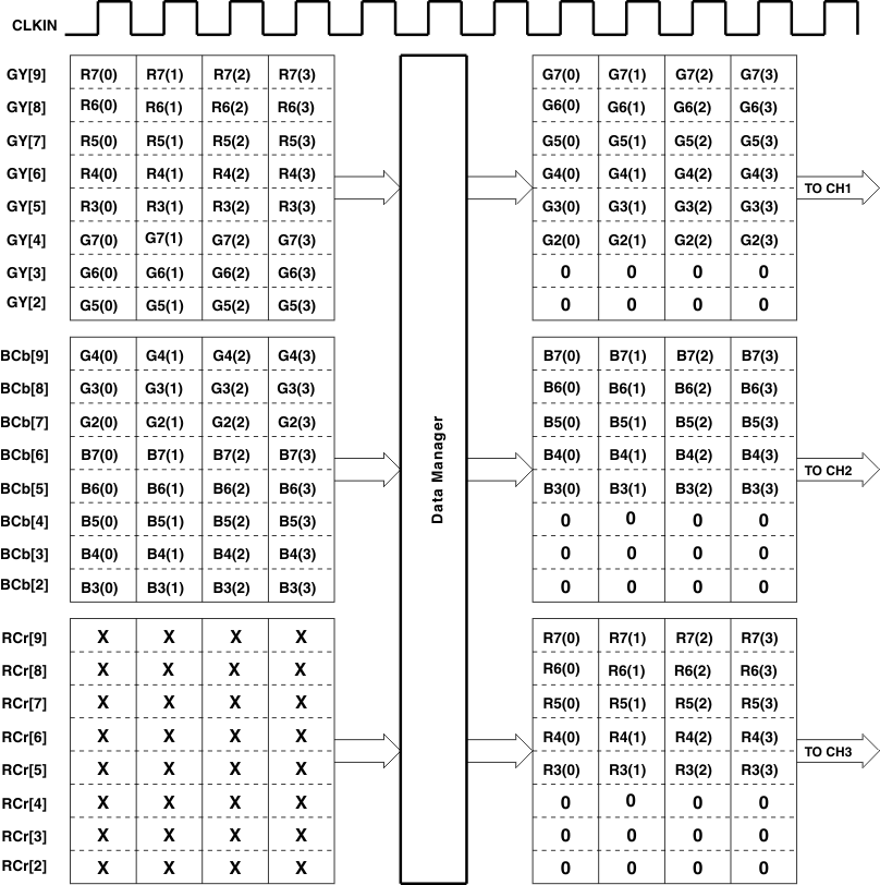 Figure 6-3 16-Bit RGB 4:4:4 Data Format
CLKIN is equal to 1x the pixel clock. This format is only supported in VESA mode and can be used for PC graphics applications that do not require full 8-bit resolution on each color component.
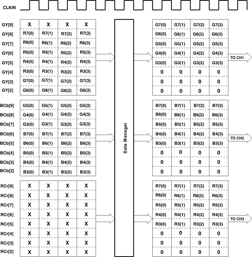 Figure 6-4 15-Bit RGB 4:4:4 Data Format
CLKIN is equal to 1x the pixel clock. This format is only supported in VESA mode and can be used for PC graphics applications that do not require full 8-bit resolution on each color component.
6.3 Clock Generator (CGEN)/Clock Driver (CDRV)
The clock generator/clock driver blocks generate all on-chip clocks for 4:2:2 to 4:4:4 and 2x video oversampling. The DMAN setting controls whether the input data is 4:2:2 or 4:4:4 sampled, and whether a 30-, 20- or 10-bit interface is used. This selection affects the clock input frequency assumed to be present on CLKIN.
- 30-bit 4:4:4: 1x pixel clock. 4:2:2 to 4:4:4 interpolation should be bypassed. Optional 2x oversampling is available for formats with pixel clock up to 80 MHz.
- 20-bit 4:2:2: 1x pixel clock. 4:2:2 to 4:4:4 interpolation should be switched in, and is available for formats with pixel clock up to 150 MHz. Optional 2x oversampling available for formats with pixel clock up to 80 MHz.
- 10-bit 4:2:2 (ITU): 1/2x pixel clock. 4:2:2 to 4:4:4 interpolation should be switched in, and is available for formats with pixel clock up to 150 MHz. Optional 2x oversampling is available for formats with pixel clock up to 80 MHz.
The internal DLL (delay-locked loop) generates the higher clock frequencies. The user should program the input frequency range selection register, dll_freq_sel, according to the frequency present on CLK_IN when using either or both interpolation/oversampling stages.
The 4:2:2 to 4:4:4 stage is switched in or bypassed, depending on the setting of data_ifir12_bypass register (interpolation only on chroma channels). This feature should only be used with YCbCr 4:2:2 input. The THS8200 can perform color space conversion to RGB depending on the CSC setting. The dtg2_rgbmode_on register should be set corresponding to the color space representation of the DAC output.
The 2x oversampling stage is switched in or bypassed, depending on the setting of data_ifir35_bypass register.
The user should not enable the 2x oversampling stage when the CLK_IN frequency exceeds 80 MHz, as is the case for the higher PC graphics formats and 1080P HDTV. In this case the DLL should be bypassed using the vesa_clk register to disable the 2x frequency generation. As explained in the detailed register map description for this register, it is still possible to support 20-bit 4:2:2 input in this mode (for example, for 1080P).
A second bypass mode operation exists for the DLL, enabled by the dll_bypass register. When this bypass mode is active, the CLKIN input is assumed to be 2x pixel frequency.
6.4 Color Space Conversion (CSC)
THS8200 contains a fully-programmable 3×3 multiply/add and 3×1 adder block that can be switched in for all video formats up to a pixel clock frequency of 150 MHz. Color space conversion is thus available for all DTV modes, including 1080P and VESA modes up to SXGA at 75 Hz (135 MSPS). The operation is done after optional 4:2:2 to 4:4:4 conversion, and thus on the 1x pixel clock video data prior to optional 2x video oversampling. The CSC block can be switched in or bypassed depending on the setting of register csc_bypass.
Each of the nine floating point multiplier coefficients of the 3×3 multiply/add is represented as the combination of a 6-bit signed binary integer part, and a 10-bit fractional part. The integer part is a signed magnitude representation with the MSB as the sign bit. The fractional part is a magnitude representation; see the following example.
The register nomenclature is: csc_<r,g,b> <i,f>c<1,2,3> where:
- <r,g,b> identifies which input channel is multiplied by this coefficient (r = red/Cr, g = green/Y,
b = blue/Cb input). - <i,f> identifies the integer (i) or fractional (f) part of the coefficient.
- <1,2,3> identifies the output channel from the color space converter: 1 = Yd/Gd, 2 = Cb/Bd, 3 = Cr/Rd.
For the offset values, a value of 1/4 of the desired digital offset needs to be programmed in the individual offset register, so a typical offset of 512 (offset over 1/2 of the video range) requires programming a value of 128 decimal into the offset<1,2,3> registers, where again <1,2,3> defines the output channel affected, with similar convention as shown previously.
Saturation logic can be switched in to avoid overflow and underflow on the result after color space conversion using the csc_uof_cntl register.
An example of how to program the CSC follows. This also explains the numeric data formats.
CSC configuration example: HDTV RGB to HDTV YCbCr
The formulas for RGB to YCbCr conversion are:
- Yd = 0.2126 × Rd + 0.7152 × Gd + 0.0722 × Bd
- Cb = −0.1172 × Rd – 0.3942 × Gd + 0.5114 × Bd + 512
- Cr = 0.5114 × Rd – 0.4646 × Gd – 0.0468 × Bd + 512
To program the red coefficient of channel 1 (Y) with the value of 0.2126 the following must be done:
- Realize that this is a positive value so the sign bit of the integer part is 0 (bit 5 of csc_ric1 = 0).
- Note that there is no integer portion of the coefficient (bit 4−bit 0 = 00000).
- The binary representation of the fractional part can be constructed directly from the binary equivalent of the fractional part multiplied by 1024 (0.2126 × 1024 = 217.7), rounded to the nearest integer (218) and represented as a binary 10-bit number (00 1101 1010).
Using the above method all the registers for the CSC blocks can be programmed with the correct value for RGB to YCbCr conversion. Below is a complete list of register values for the above conversion.
| 0.2126 → csc_ric1 = 00 0000 | csc_rfc1 = 00 1101 1010 |
| 0.7152 → csc_gic1 = 00 0000 | csc_gfc1 = 10 1101 1100 |
| 0.0722 → csc_bic1 = 00 0000 | csc_bfc1 = 00 0100 1010 |
| −0.1172 → csc_ric2 = 10 0000 | csc_rfc2 = 00 0111 1000 |
| −0.3942 → csc_gic2 = 10 0000 | csc_gfc2 = 01 1001 0100 |
| 0.5114 → csc_bic2 = 00 0000 | csc_bfc2 = 10 0000 1100 |
| 0.5114 → csc_ric3 = 00 0000 | csc_rfc3 = 10 0000 1100 |
| −0.4646 → csc_gic3 = 10 0000 | csc_gfc3 = 01 1101 1100 |
| −0.0468 → csc_bic3 = 10 0000 | csc_bfc3 = 00 0011 0000 |
For the offsets necessary in the second and third equation, the csc_offset<n> registers need to be programmed. Add 512 to the Cb and Cr channels. The value to be programmed is 1/4 of this offset in a signed magnitude representation, thus 128 or csc_offset2 = csc_offset3 = 00 1000 0000.
Packing these individual registers into the I2C register map, the programmed values are:
| SUBADDRESS | REGISTER NAME | VALUE |
|---|---|---|
| 0x04 | csc_r11 | 0000 0000 |
| 0x05 | csc_r12 | 1101 1010 |
| 0x06 | csc_r21 | 1000 0000 |
| 0x07 | csc_r22 | 0111 1000 |
| 0x08 | csc_r31 | 0000 0010 |
| 0x09 | csc_r32 | 0000 1100 |
| 0x0A | csc_g11 | 0000 0010 |
| 0x0B | csc_g12 | 1101 1100 |
| 0x0C | csc_g21 | 1000 0001 |
| 0x0D | csc_g22 | 1001 0100 |
| 0x0E | csc_g31 | 1000 0001 |
| 0x0F | csc_g32 | 1101 1100 |
| 0x10 | csc_b11 | 0000 0000 |
| 0x11 | csc_b12 | 0100 1010 |
| 0x12 | csc_b21 | 0000 0010 |
| 0x13 | csc_b22 | 0000 1100 |
| 0x14 | csc_b31 | 1000 0000 |
| 0x15 | csc_b32 | 0011 0000 |
| 0x16 | csc_offs1 | 0000 0000 |
| 0x17 | csc_offs12 | 0000 1000 |
| 0x18 | csc_offs23 | 0000 0010 |
| 0x19 | csc_offs3 | 0000 0000 |
CSC configuration example: HDTV YCbCr to HDTV RGB
- Gd = –0.4577 × Cr + Yd – 0.1831 × Cb +328 (= 0.6408 × 128 × 4)
- Bd = 0 × Cr + Yd + 1.8142 × Cb – 929 (= −1.8142 × 128 × 4)
- Rd = 1.5396 × Cr +Yd +0 × Cb – 788 (= −1.5396 × 128 × 4)
In a similar manner, it can be calculated that the programming array is in this case:
| SUBADDRESS | REGISTER NAME | VALUE |
|---|---|---|
| 0x04 | csc_r11 | 1000 0001 |
| 0x05 | csc_r12 | 1101 0101 |
| 0x06 | csc_r21 | 0000 0000 |
| 0x07 | csc_r22 | 0000 0000 |
| 0x08 | csc_r31 | 0000 0110 |
| 0x09 | csc_r32 | 0010 1001 |
| 0x0A | csc_g11 | 0000 0100 |
| 0x0B | csc_g12 | 0000 0000 |
| 0x0C | csc_g21 | 0000 0100 |
| 0x0D | csc_g22 | 1000 0000 |
| 0x0E | csc_g31 | 0000 0100 |
| 0x0F | csc_g32 | 0000 0000 |
| 0x10 | csc_b11 | 1000 0000 |
| 0x11 | csc_b12 | 1011 1011 |
| 0x12 | csc_b21 | 0000 0111 |
| 0x13 | csc_b22 | 0100 0010 |
| 0x14 | csc_b31 | 0000 0000 |
| 0x15 | csc_b32 | 0000 0000 |
| 0x16 | csc_offs1 | 0001 0100 |
| 0x17 | csc_offs12 | 1010 1110 |
| 0x18 | csc_offs23 | 1000 1011 |
| 0x19 | csc_offs3 | 0001 0100 |
6.5 Clip/Shift/Multiplier (CSM)
There are limits on the code range of the video data if sampled according to ITU or SMPTE standards. In other words, the full 10-bit range [0:1023] is not used to represent video pixels. For example, typically 64 decimal is the lowest code allowed to represent a video signal and corresponds to the blanking level. Similarly for Y, typically the maximum code is 940 decimal. Excursions outside this range can be the result of digital video processing.
THS8200 can handle such instantaneous excursions in either of two ways: by limiting the input codes to programmable max/min values, or by allowing such excursions to occur.
Depending on which approach is chosen, the user can scale up the video data in the CSM to make sure the full-scale dynamic range of the DAC is used for optimal performance when using limiting. Alternatively, the instantaneous excursions outside the code range can be output by the DAC in the analog output signal (allowing super-white/black in analog output) when this clipping is disabled.
The CSM block allows the user to specify the behavior of THS8200 with such reduced-swing input video codes. It consists of the following:
- An optional clipping of the input video data at a high and low limit, where the limits are individually programmable per channel.
- A downward shift of the input video data, where the shift amount is individually programmable per channel.
- A multiply (magnitude scaling) function of the video data, where the multiplier coefficient is individually programmable per channel.
6.5.1 Clipping
Clipping (limiting) of the video input data can be turned on or off on a per-channel basis, and selectively at the high and/or low end, by programming the csm_<gy,rcr,bcb>_<high,low>_clip_on registers. The high/low clipping values can be programmed on a per-channel basis using registers csm_clip_<gy,rcr,bcb>_<high,low>.
Figure 6-5 shows a typical situation to clip ITU-R.BT601 sampled video signals.
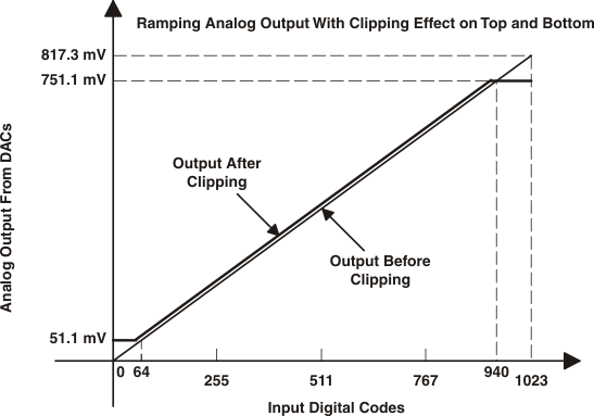 Figure 6-5 Effect of Clipping on Analog Output
6.5.2 Shifting
Next the video data can be shifted over a programmable amount downward. The number of codes over which to shift the input video data is set per channel by programming csm_shift_<gy,rcr,bcb>. Shifting of the input video data can be done downwards over 0..255 codes inside the CSM.
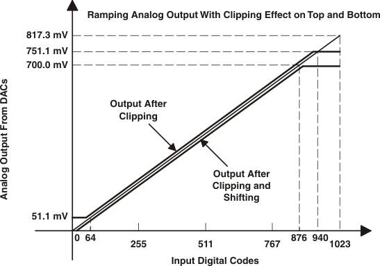 Figure 6-6 Effect of Shifting on Clipped Analog Output
Figure 6-5 and Figure 6-6 also show the analog output from the DAC if the full-scale video range over the [64..940] input would correspond to the normal 700-mV range for component video. This full-scale range is set by the selected FSADJ full-scale setting (register data_fsadj).
6.5.3 Multiplying
When the 10-bit range is not fully used for video, scale the input video data to use the full 10-bit dynamic range of the DACs. Care should be taken not to overflow/underflow the available range after scaling.
This multiplying control serves two purposes:
- Use of the full 10-bit DAC range for inputs of reduced range.
- Individual fine gain control per channel to compensate for gain errors and provide white balance control.
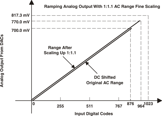 Figure 6-7 Effect of Scaling the Analog Video Output
Figure 6-7 illustrates a shifted analog ramping output. The multiplication factor could be calculated to scale this output range to the full 10-bit range of the DAC. Note that this scaling can be programmed individually per channel using registers csm_mult_<gy,rcr,bcb>. The range of the multiplication is 0..1.999, coded as a binary weighted 11-bit value, thus: csm_mult_<gy,rcr,bcb> = (Desired scale ( 0 to 1.999) / 1.999) × 2047.
Note that this approach allows to scale input code ranges that are different on each channel to an identical full-scale DAC output compliance, as is required for ITU-R.BT601 sampled signals where Y video data is represented in the range [64..940] and both Cb,Cr color difference channels are coded within the range [64..960]. All three channels need to generate a 700-mV nominal analog output compliance. Using a combination of FSADJ—adjusting the full-scale current of all DAC channels simultaneously in the analog domain—and digital CSM control, different trade-offs can be made for DAC output amplitude control, including channel matching.
As discussed in Section 6.7, the user also controls the DAC output levels during blanking, negative and positive sync, pre- and post-equalization, and serration pulses. Using a combination of CSM and DTG programming, it is therefore possible to accommodate many video standards, including those that require a video blank-to-black level setup, as well as differing video/sync ratios (for example, 10:4 or 7:3).
Finally, using the selectable full-scale adjustment from the FSADJ1 or FSADJ2 terminals, it is possible to switch between two analog output compliance settings with no hardware changes.
Physically, the CSM output is represented internally as an 11-bit value to improve the DAC linearity at the 10-bit level after scaling. Each DAC internally is of 11-bit resolution.
6.6 Interpolating Finite Impulse Response Filter (IFIR)
For relaxing the requirements of the reconstruction filter behind the DAC in the analog domain, and to take advantage of the high-speed capability of the DACs in THS8200, a 2x digital up-sampling and interpolation filter module is integrated.
Figure 6-8 through Figure 6-11 show the YRGB and CbCr filtering requirements for HDTV (SMPTE274M/296M standards) and SDTV (ITU-R.BT601 standard), respectively.
 Figure 6-8 PB and PR Filter Requirements Based on SMPTE 296M/274M
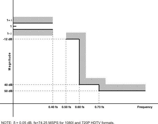 Figure 6-9 Y and RGB Filter Requirements Based on SMPTE 296M/274M
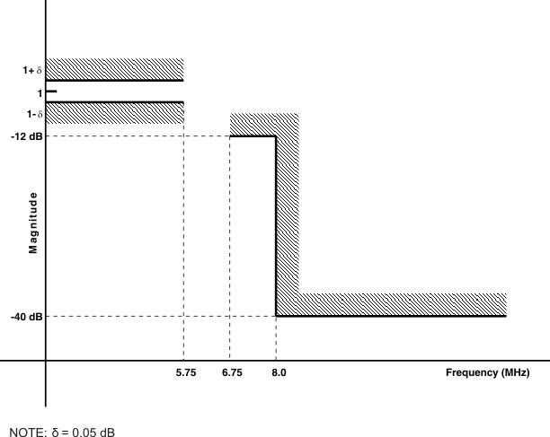 Figure 6-10 Y and RGB Filter Requirements Based on ITU-R.BT601
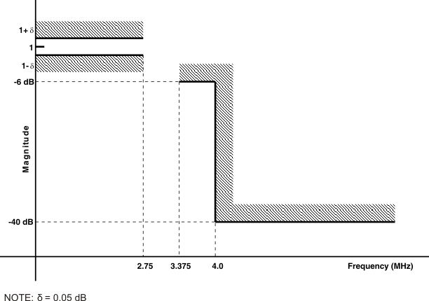 Figure 6-11 Cb and Cr Filter Requirements Based on ITU-R.BT601
Figure 6-12 through Figure 6-14 illustrate the frequency and phase responses of the interpolating filters. The actual response using the finite-word length coefficients present in THS8200 is shown. The same filter characteristic is used for SDTV/HDTV modes and for both 4:2:2 to 4:4:4 interpolation (2 filters, one on each of Cb and Cr channels, switched in when a 4:2:2 input mode is selected on DMAN to interpolate chrominance from 1/2 to 1x pixel clock rate) as well as for 2x video oversampling (3 filters, one on each DAC channel, switched in when 2x interpolation is activated).
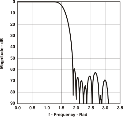 Figure 6-12 IFIR Frequency Response
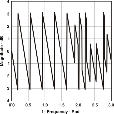 Figure 6-14 IFIR Phase Response
 Figure 6-13 IFIR Pass-Band Frequency Response
Each of the two interpolation stages can be switched in or bypassed:
- Register data_ifir12_bypass controls the 4:2:2 to 4:4:4 filter bank (these filters should be set active when a 4:2:2 input mode is selected on DMAN).
- Register data_ifir35_bypass controls the 1x to 2x interpolation stage and can be set active for optional 2x interpolation when an input format with pixel clock < 80 MSPS is present.
6.7 Display Timing Generator (DTG)
6.7.1 Overview of Functionality
THS8200 can generate dedicated Hsync/Vsync/FieldID video synchronization outputs, as well as a composite sync inserted on either the G/Y or all analog output channels. Both types of output synchronization can be available simultaneously and programmed independently. Synchronization patterns are fully programmable to accommodate all standard VESA (PC graphics) and ATSC (DTV) formats as well as nonstandard formats.
For the purpose of output video timing generation, the device is configured in HDTV, SDTV or VESA mode (dtg1_mode register). Depending on the selected DTG mode, a number of line types are available to generate the full video frame format. The timing and position of horizontal and vertical syncs, the position of horizontal and vertical blanking intervals, and the structure, position and width of equalization pulses, pre- and post-serration pulses within the vertical blanking interval are user-programmable.
The DTG determines:
- the frame format/field format (number of pixels/line, number of lines/field1, number of lines/field2, number of fields/frame = 1 for progressive or 2 for interlaced formats) and its synchronization to the input data source.
- Registers: dtg1_total_pixels, dtg1_linecnt, dtg1_frame_size, dtg1_field_size
- in slave mode, whether HS_IN, VS_IN, FID (dedicated sync inputs) are used for input video synchronization or video timing is extracted from embedded SAV/EAV codes, as well as the relative position of the video frame with respect to these synchronization signals.
- Registers: dtg2_embedded_timing, dtg2_hs_in_dly, dtg2_vs_in_dly
- the I/O direction of the HS_IN and VS_IN input signals (master vs slave mode), and the polarity of the HS_IN, VS_IN, and FID signals.
- Registers: dtg2_hs_pol, dtg2_vs_pol, dtg2_fid_pol
- the position and width of the HS_OUT, VS_OUT output signals, and their polarity.
- Registers: dtg2_hlength, dtg2_hdly, dtg2_vlength1, dtg2_vdly1, dtg2_vlength2, dtg2_vdly2, dtg2_vsout_pol, dtg2_hsout_pol
- field reversal within DTG.
- Register: dtg1_field_flip
- the active video window: width and position of horizontal blanking interval, width and position of vertical blanking interval.
- Registers: dtg2_bp<n>, dtg2_linetype<n> and the dtg1_spec_x registers, see DTG Line Type Overview (Section 6.7.3).
- the composite sync format: horizontal line timing includes serration, interlaced sync and broad pulses on each line in vertical blanking interval, width of vertical sync.
- Registers: dtg1_mode, dtg1_spec_<a,b,c,d,d1,e,g,h,i,k,k1>
- the behavior of the composite sync insertion: inserted on G/Y-channel only, or inserted on all channels, or no composite sync insertion; the amplitudes of the inserted negative and positive sync, the amplitudes of all serration pulses and broad pulses during the vertical blanking interval.
- Registers: dtg1_<y,cbcr>_sync_high, dtg1_<y,cbcr>_sync_low
- the DAC output amplitude during blanking and whether video data is passed or not during the active video portion of lines within the vertical blanking interval that contain no vertical sync, serration, or broad pulses.
- Registers: dtg1_<y,cbcr>_blank, dtg1_pass_through
- the width of each color bar of the color bar test pattern.
- Registers: dtg1_vesa_cbar_size
6.7.2 Functional Description
The user should program the DTG with the correct parameters for the current video format. The DTG contains a line and a pixel counter, and a state machine to determine which user−defined line waveform to output for each line on the analog outputs. The pixel counter counts horizontally up to the total number of pixels per line, programmed in 'dtg1_total_pixels'. The line counter counts up to 'dtg1_field_size' lines in the first field, and continues its count up to 'dtg1_frame_size' lines in the total frame (field1+field2).
The current field is derived from the even/odd field ID signal, which is sampled at the start of the Vsync period. The source for the internal FID signal can be either the signal to the FID terminal, or can be internally derived from relative Hsync/Vsync alignment on the corresponding terminals, as selected by 'dtg2_fid_de_cntl' and the current DTG mode (VESA vs. SDTV/HDTV). See register map description of 'dtg2_fid_de_cntl' for more details. Derivation of FID from Hsync/Vsync input alignment is done according to the EIA−861 specification. There is a tolerance implemented on Hsync/Vsync transition misalignment. When the active edge of the Vsync transition occurs within ±63 clock cycles from the active edge of Hsync, both signals are interpreted as aligned, which signals field 1. Because of this timing window, the internal FieldID signal is generated later than the start of Vsync period. Since the signal is internally sampled at the start of the Vsync period to determine the current field, the field interpretation is opposite. Use the 'field_flip' register to correct this through field reversal.
If the video format is progressive, only field1 exists and no FID signal is needed. However the DTG will only startup when a field 1 condition is detected i.e when FID is detected low at the start of the Vsync period. Thus in the case of a progressive video format, and when using the device with external FID input, the user must make sure to keep the FID terminal low.
It is also needed for proper DTG synchronization that the programmed Hsync and Vsync input polarities are correct. Since Hsync, Vsync polarities change for different VESA PC formats, the device has built−in support to detect the incoming sync polarities. This is done by comparing the width of Hsync high ('misc_ppl') to the total line length ('dtg2_pixel_cnt') to derive the Hsync duty cycle and thus its polarity. Upon this detection, the user can program the detected incoming polarity for DTG input synchronization ('dtg2_hs_pol') – it is not set automatically by the device. The procedure is similar for Vsync polarity detection, using registers 'misc_lpf', 'dtg2_line_cnt' and 'dtg2_vs_pol'.
The DTG synchronization can be separated into three functions:
- Internal synchronization: How the DTG is synchronized with respect to the internal horizontal and vertical counters.
- Source synchronization: How the horizontal and vertical counters are synchronized to the HS_IN/VS_IN/FID or SAV/EAV signals.
- Output synchronization: how the output timings HS_OUT, VS_OUT, and the composite sync output are synchronized to the DTG and the horizontal and vertical counters.
The DTG is based on a state machine that can generate a set of line types which can override the values on the DAC inputs. The DTG output is multiplexed into the data path by the DIGMUX. The selected video format preset setting, or the programmed (line type, breakpoint) table in case a generic mode is selected in dtg1_mode, determines which line type is generated for a particular line, and where this DTG output is used to override the normal DAC inputs. Internally, a fixed preconfigured number of line types exists from which the user can select.
Also, for each set of line types (there are two different sets of line types possible) the user can program the horizontal duration of each predefined excursion (negative sync, positive sync, back porch, front porch, broad pulse, interlaced sync, etc.) and also the amplitude (for example, negative sync amplitude, positive sync amplitude, blank amplitude).
The setting of dtg1_mode determines:
- Internal synchronization: The 0H reference (horizontal reset of the DTG) is different between SDTV and HDTV.
- Output synchronization: The available set of output synchronization line types depends on these modes. The user can choose from a number of predefined line types for each mode. In each mode, the user is able to program the timings along the line. However some timings are hard coded by the selected DTG_mode (for example, rise/fall times for sync are different; see DTG Line Type Overview, Section 6.7.3) and not all line types can be selected in each DTG mode (for example, HDTV allows tri-level sync, while SDTV only allows generation of bi-level negative syncs).
6.7.2.1 Predefined DTG Video Formats (Presets)
While the DTG has the flexibility to generate a wide array of video output formats and their synchronization signals, the most common video formats have predefined settings for the field and frame sizes and for (line type, breakpoint) settings.
When selecting a video format preset, the horizontal timings of the line types still need to be programmed. The preset only fixes the (line type, breakpoint) table.
6.7.2.2 Internal Synchronization
The pixel and line counters of the DTG are reset by internal signals. In slave mode (THS8200 slaves to external video input source) these signals are derived from either the embedded SAV/EAV codes or the dedicated Hsync/Vsync/FID inputs. In master mode, these counters are in free-run and the HS_IN/VS_IN signals are generated by the THS8200 based on the programmed field/frame parameters. Master mode is only available for progressive-scan VESA modes. FID is not generated in master mode.
The user can delay, in both horizontal and vertical directions, the 0-reference of the DTG by programming the input delay registers. Physically, the horizontal and vertical DTG startup values are altered. The effect is that, when a vertical or horizontal sync is received, either from dedicated inputs or from embedded SAV/EAV codes, the output frame starts at position (x,y). This ensures that, for example, the output video frame can be centered on the display.
Based on the 0-reference of the DTG, the line types are generated and the DIGMUX will select between the video input and the DTG output for each line type. All horizontal timings of the different line types are programmable, including the portion of the video line seen as active video. A complete overview of all available line types in either SDTV or HDTV mode is presented in Section 6.7.3.
Additionally, Hsync/Vsync outputs can be generated, synchronized to the THS8200 DAC outputs. These outputs are programmable in width, position and polarity, based on the horizontal/vertical pixel counters, and thus independently of the DTG reference. This ensures that independent synchronization is possible between the composite sync output inserted into the DAC output(s) and the dedicated Hsync/Vsync outputs. Because of their programmability, these output signals could be used for other purposes as well; for example, Vsync could be programmed as a signal active during the VBI.
Figure 6-15 shows how the internal pixel and line counters are synchronized to internal HS and VS signals in slave mode. HS and VS are internal signals derived from either HS_IN, VS_IN, or from embedded SAV/EAV codes in the input video data. Since the 0-reference of the DTG is determined by these counters, the dtg2_vs_in_dly and dtg2_hs_in_dly register settings influence both HS_OUT, VS_OUT and composite sync output timing. The dtg2_vdly<1,2> and dtg2_hdly settings, on the other hand, only affect HS_OUT and VS_OUT, because they are downstream of the pixel counter. Likewise, dtg2_hlength and dtg2_vlength<1,2> only affect these dedicated sync output signals.
 Figure 6-15 THS8200 DTG VS/HS Output Generation
Note that both independent sets of delay registers allow accommodation of different input timing references in slave mode. When the device is configured in master mode, the delay registers can compensate for different external (frame memory) synchronization requirements.
6.7.2.3 Output Synchronization: Composite Sync
The composite sync is generated from a programmed sequence of (line type, breakpoint) combinations, either user-programmed (in generic mode) or preset (in preset mode). The line type determines the waveform shape at the output of the DAC(s) with programmable amplitudes and timings.
On each line, at the horizontal reference point of the DTG, the DTG decides where to start/stop the DTG-generated data and where to pass input video data. For example, during an active video line, ancillary data can be embedded in the digital stream outside the active video portion of the line, that it might be necessary to convert to analog. Alternatively, during a nonactive video line, where normally the predefined line type would be inserted, ancillary data might need to be passed during the active video portion of the line.
The amplitudes of positive, negative sync excursions and of the negative serration, pre- and post-equalization and broad pulses are independently programmable between G/Y and BPb, RPr channels. Therefore sync insertion can be programmed on only the G/Y output or on all DAC outputs.
To limit the number of selection bits to select the line type, and because of the fact that a set of line types can be defined that is mutually exclusive for SDTV and HDTV video modes, there are two DTG video modes: SDTV and HDTV. There is a third DTG mode (VESA) which does not use the line type/breakpoint state machine and only generates Hsync/Vsync outputs.
6.7.2.4 Output Synchronization: Hsync/Vsync Outputs
These are the HS_OUT and VS_OUT signals, of which the width, position and polarity are programmable in all DTG modes.
6.7.3 DTG Line Type Overview
6.7.3.1 HDTV Mode
When an HDTV mode is selected in dtg1_mode (preset or generic), a tri-level sync is inserted on the analog output at the start of every video line. The amplitudes during negative and positive excursions are programmable, as well as the horizontal timing parameters (width, position) of both excursions.
The transition time for negative-to-blank and blank-to-positive excursions during VBI is fixed to 2T, generating a tri-level sync negative-to-positive excursion of 4T. The line type is programmed in registers dtg2_linetype<n> and is output by the DTG from the vertical field/frame position corresponding to the line number programmed in register dtg2_breakpoint<n>, until the line number listed in the next breakpoint register is reached. An example for 1080I is shown in Figure 6-25.
The DTG overrides the input video data except where specified below for the specific line types.
The horizontal timings shown in Figure 6-16 and Figure 6-17 correspond to the dtg1_spec_<x> registers. Note that the f spec is fixed.
 Figure 6-16 Tri-Level Line-Synchronizing Signal Waveform
 Figure 6-17 THS8200 VBI Line Types in HDTV Mode
6.7.3.2 Active Video
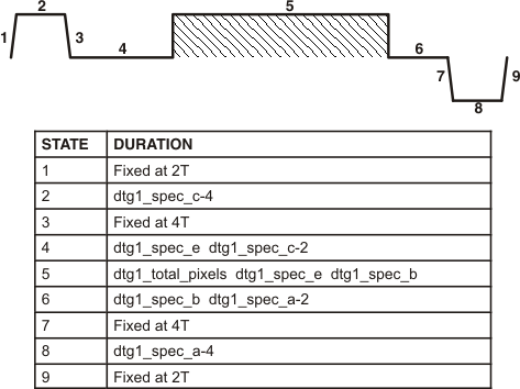 Figure 6-18 HDTV Line Type ACTIVE_VIDEO
6.7.3.3 FULL NTSP (Full Normal Tri-Level Sync Pulse)
Device input data is passed during state #5 if dtg1_pass_through is on.
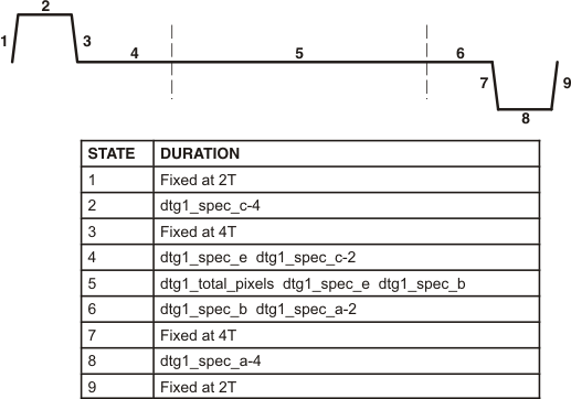 Figure 6-19 HDTV Line Type FULL_NSTP
6.7.3.4 NTSP NTSP (Normal Tri-Level Sync Pulse/Normal Tri-Level Sync Pulse)
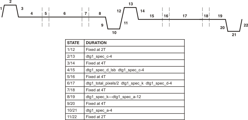 Figure 6-20 HDTV Line Type NTSP_NTSP
6.7.3.5 BTSP BTSP (Broad Pulse and Tri-Level Sync Pulse/Broad Pulse and Tri-Level Sync Pulse)
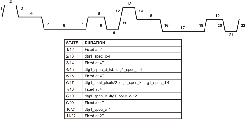 Figure 6-21 HDTV Line Type BTSP_BTSP
6.7.3.6 NTSP BTSP (Normal Tri-Level Sync Pulse/ Broad Pulse and Tri-Level Sync Pulse)
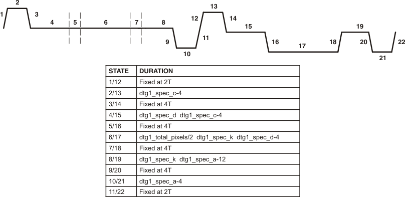 Figure 6-22 HDTV Line Type NTSP_BTSP
6.7.3.7 BTSP NTSP (Broad Pulse and Tri-Level Sync Pulse/Normal Tri-Level Sync Pulse)
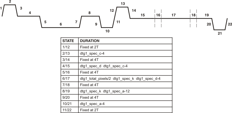 Figure 6-23 HDTV Line Type BTSP_NTSP
6.7.3.8 Full BTSP (Full Broad Pulse and Tri-Level Sync Pulse)
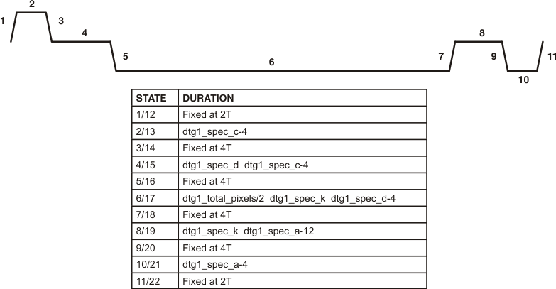 Figure 6-24 HDTV Line Type FULL_BTSP
Example: 1080I/P
THS8200 is put into 1080I mode by programming dtg1_mode = 0001. Figure 6-25 shows the required output format of both fields for 1080I and 1080P.
When in 1080I preset mode, the (line type, breakpoint) table and frame and field size registers are filled out as follows internally:
| Breakpoints | Line Type | |
| 6 | BTSP_BTSP | |
| 7 | NTSP_NTSP | |
| 21 | FULL_NTSP | |
| 561 | ACTIVE_VIDEO | |
| 563 | FULL_NTSP | |
| 564 | NTSP_BTSP | |
| 568 | BTSP_BTSP | |
| 569 | BTSP_NTSP | |
| 584 | FULL_NTSP | |
| 1124 | ACTIVE_VIDEO | |
| 1126 | FULL_NTSP | |
| frame_size = 10001100101; 1125d | ||
| field_size = 01000110011; 563d | ||
From line 1 to 5, line type BTSP_BTSP is generated. When the line counter reaches line 6, the DTG switches to line type NTSP_NTSP, etc. Note that the dtg1_spec_<x> registers need to be filled out with the correct values to set the horizontal line timings.
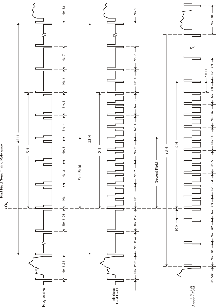 Figure 6-25 Field/Frame Synchronizing Signal Waveform (1080I and 1080P Formats)
6.7.3.9 SDTV Mode
In SDTV mode, the start of a video line is signaled by the leading edge of a negative-going bi-level sync.
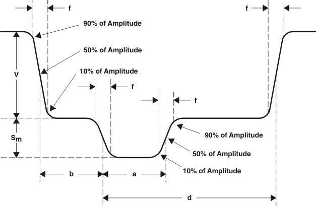 Figure 6-26 Horizontal Synchronization Signal Waveform
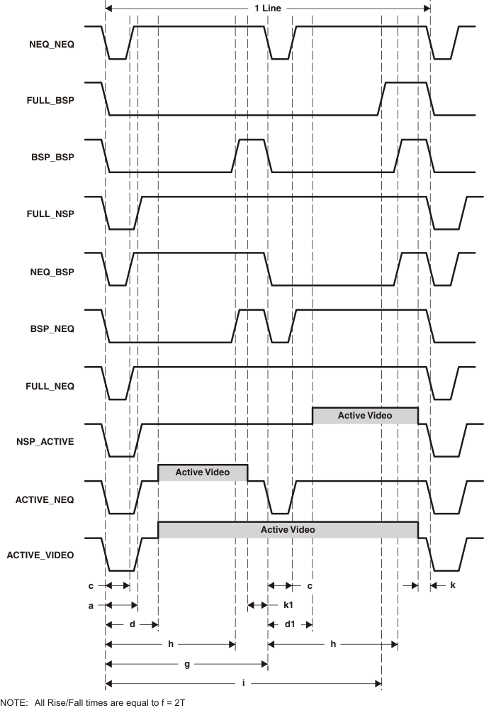 Figure 6-27 THS8200 VBI Line Types in SDTV Mode
6.7.3.10 NEQ_NEQ (Negative Equalization Pulse/Negative Equalization Pulse)
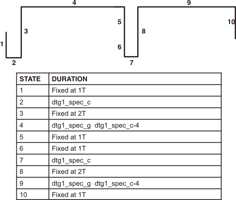 Figure 6-28 SDTV Line Type NEQ_NEQ
6.7.3.11 FULL_BSP (Full Broad Sync Pulse)
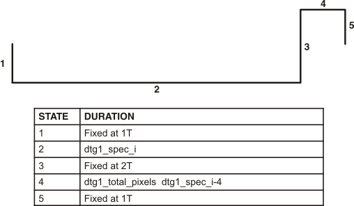 Figure 6-29 SDTV Line Type FULL_BSP
6.7.3.12 BSP_BSP (Broad Sync Pulse/Broad Sync Pulse)
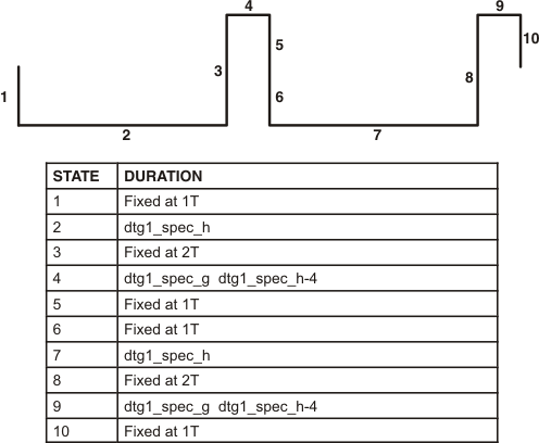 Figure 6-30 SDTV Line Type BSP_BSP
6.7.3.13 FULL_NSP (Full Normal Sync Pulse)
Device input data is passed during states number 4 and number 5 if dtg1_pass_through is on.
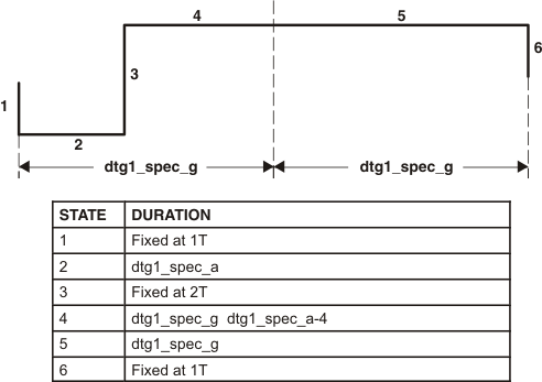 Figure 6-31 SDTV Line Type FULL_NSP
6.7.3.14 NEQ_BSP (Negative Equalization Pulse/Broad Sync Pulse)
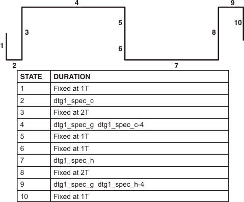 Figure 6-32 SDTV Line Type NEQ_BSP
6.7.3.15 BSP_NEQ (Broad Sync Pulse/Negative Equalization Pulse)
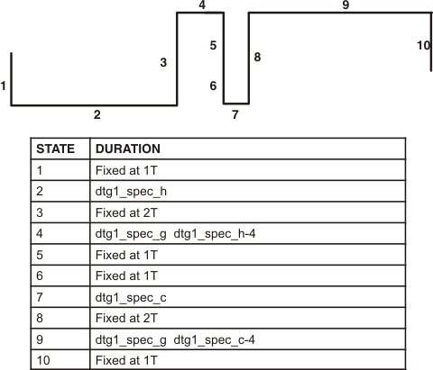 Figure 6-33 SDTV Line Type BSP_NEQ
6.7.3.16 FULL_NEQ (Full Negative Equalization Pulse)
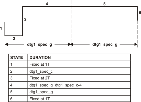 Figure 6-34 SDTV Line Type FULL_NEQ
6.7.3.17 NSP_ACTIVE (Normal Sync Pulse/Active Video)
Video data is always passed during state number 5.
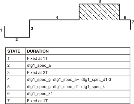 Figure 6-35 SDTV Line Type NSP_ACTIVE
6.7.3.18 ACTIVE_NEQ (Active Video/Negative Equalization Pulse)
Video data is always passed during state number 5.
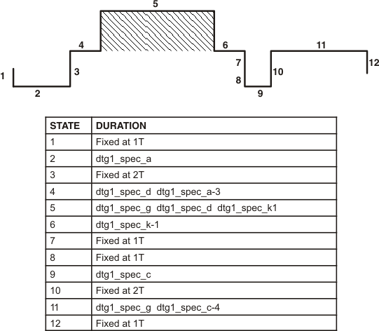 Figure 6-36 SDTV Line Type ACTIVE_NEQ
6.7.3.19 ACTIVE VIDEO
Video data is always passed during state number 5.
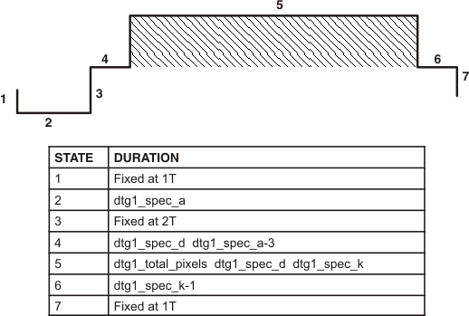 Figure 6-37 SDTV Line Type ACTIVE_VIDEO
Example:525I
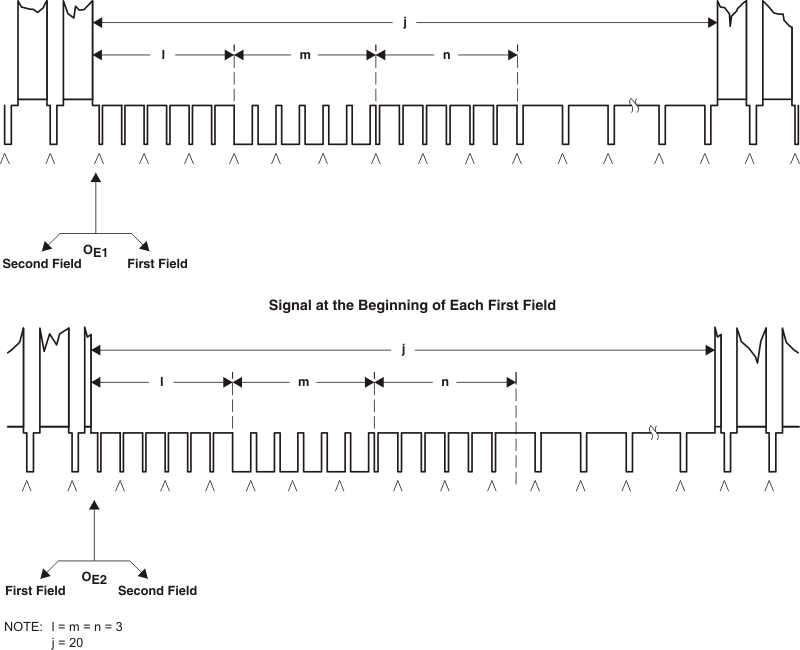 Figure 6-38 Field/Frame Synchronizing Signal Waveform (525I Format)
When the 525I preset is selected, the following line type sequence is active:
| Breakpoints | Line Type | |
| 4 | NEQ_NEQ | |
| 7 | BSP_BSP | |
| 10 | NEQ_NEQ | |
| 20 | FULL_NSP | |
| 263 | ACTIVE_VIDEO | |
| 264 | ACTIVE_NEQ | |
| 266 | NEQ_NEQ | |
| 267 | NEQ_BSP | |
| 269 | BSP_BSP | |
| 270 | BSP_NEQ | |
| 272 | NEQ_NEQ | |
| 273 | FULL_NEQ | |
| 282 | FULL_NSP | |
| 283 | NSP_ACTIVE | |
| 526 | ACTIVE_VIDEO | |
| frame_size = 1000001101; 525d | ||
| field_size = 00100000111; 263d | ||
It can be seen this corresponds to the frame format shown, with 263 lines in digital field1 and 262 lines in digital field2.
6.8 D/A Conversion
THS8200 contains three DACs with an internal resolution of 11 bits, and maximum speed of 205 MSPS. This allows operation with all (H)DTV formats including 1080P, and PC graphics formats up to UXGA at 75 Hz.
The DAC output compliance can be selected between two full-scale ranges using the data_fsadj register. DIGMUX selects DTG output data during nonvideo line types, except when dtg1_passthrough is active: in this case video input data still is passed during the active video portion of certain line types, as identified in Section 6.7.3 on the DTG line types.
THS8200 supports output in either RGB or YPbPr color spaces. When using RGB output, the dtg2_rgb_mode_on register needs to be set. In this case an offset is added to all DAC output channels to provide headroom for the negative sync. Nominally the blanking level is at 350 mV, and the 700 mV swing extends upwards. Therefore peak white corresponds to 1.05 V. When YPbPr mode is selected on this register, the offset is only added to the Y channel output; Pb and Pr outputs now have a video range from 0 to 700 mV with 0 V corresponding to internal DAC input code 0 (note that due to the CSM block this could correspond to another device input code). The Cb and Cr chroma difference channels are thus assumed to be offset binary encoded, not 2s complement.
Finally, the DTG mode determines whether the DIGMUX switches in output data from the DTG. For example, in VESA mode the DACs are always driven by the video input bus. When the DTG overrides the video input bus in SDTV or HDTV modes, the actual amplitude levels output by the DACs during this time are user-programmable using the dtg1_<y,cbcr>_blank , dtg1_<y, cbcr>_sync_low, and dtg1_<y, cbcr>_high registers.
The following sections described some of the analog component video output formats that can be generated from THS8200.
6.8.1 RGB Output Without Sync Signal Insertion/General-Purpose Application DAC
In this mode, no sync signal is inserted on any of the analog outputs. HS_OUT and VS_OUT signals are generated for output video synchronization. This mode is commonly used in computer graphics video output.
Two levels of full-scale output can be selected by software. For video applications, the nominal voltage levels are 0.7 V and 1.305 V.
For component video applications, the nominal voltage level is 0.7 V; 1.305 V is used in NTSC/PAL composite video display. For composite video applications, the digital video stream must be encoded in an external digital NTSC/PAL encoder. The THS8200 only converts the digital composite signal to analog composite video. Figure 6-39 illustrates analog outputs without sync insertion.
When the THS8200 is programmed in this mode, it can also be used as a general-purpose DAC due to the linear response to the DAC input codes. Optionally, the CSM block can be bypassed to avoid any processing on the device input codes.
 Figure 6-39 RGB Without Sync Insertion or Composite Video Output
Figure 6-40 shows the linear DAC I/O relationship for either of the two nominal full-scale settings.
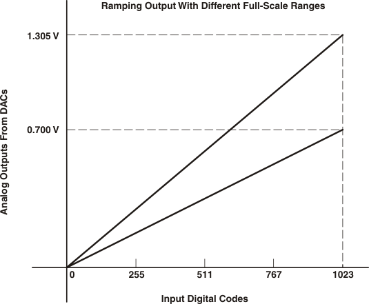 Figure 6-40 Ramping Output With Different Full-Scale Ranges
6.8.2 SMPTE-Compatible RGB Output With Sync Signal Inserted on G (Green) Channel
In this mode, a tri-level (HDTV modes)/bi-level (SDTV modes) sync signal is inserted into the G channel. The nominal analog output voltage range, which is from the sync tip to the peak of active video, is from 0.0 V to 1.050 V. During the active video period, the peak-to-peak ac value (dynamic range) is 700 mV (from 350 mV to 1050 mV). The blank levels on all three channels correspond to the bottom code 64 and are at 350 mV. Figure 6-41 and Figure 6-42illustrate the analog video output signals, both the output from the G channel with a tri-level or a bi-level sync pulse inserted, as well as the outputs from R and B channels. No sync signal is inserted during the sync period on R and B channels.
Alternatively, sync can be inserted on all three channels on THS8200 by appropriately programming the sync amplitude levels. On those channels where no sync is inserted, the blank levels are maintained at a 350-mV dc level.
The range of active video codes on the R, G, and B channels is from 64 to 940. By definition, code 64 corresponds to blank-level output, and code 940 corresponds to peak analog output. Input codes outside this region can either be clipped by THS8200 or can be passed, depending on the CSM setting. When passed, the user should make sure not to overdrive the DAC outputs outside the DAC output compliance range if instantaneously high output codes would occur.
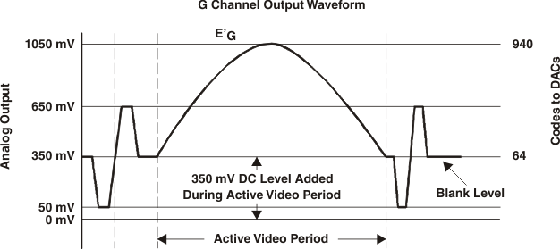 Figure 6-41 G-Channel Output Waveform
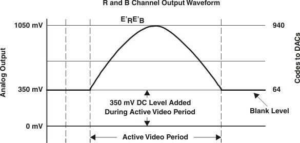 Figure 6-42 R- and B-Channel Output Waveform
6.8.3 SMPTE-Compatible Analog-Level Output With Sync Inserted on All RGB Channels
This is another SMPTE-compatible RGB output. This mode is very similar to the mode described in Section 6.8.2, except the sync signals are inserted on all three channels. Now all three channels have the same analog output format, during both the active video period and the sync period.
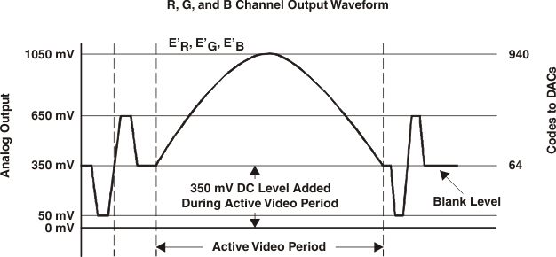 Figure 6-43 R-, G-, and B-Channel Output Waveform
6.8.4 SMPTE-Compatible YPbPr Output With Sync Signal Inserted on Y Channel Only
In this mode, the output color space is YCrCb. The sync signal is inserted on the Y channel only.
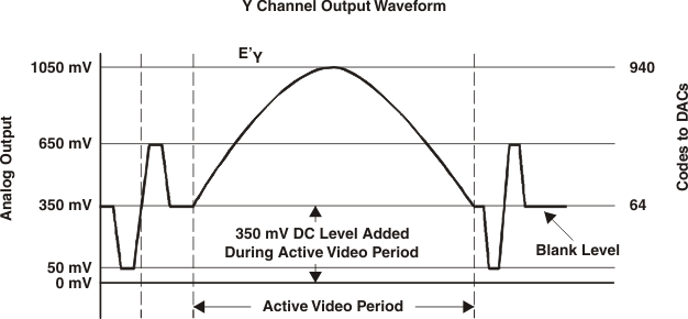 Figure 6-44 Y-Channel Output Waveform
The input code range of the Y channel is from 64 to 940, but the range of input codes of Cr and Cb is from 64 to 960.
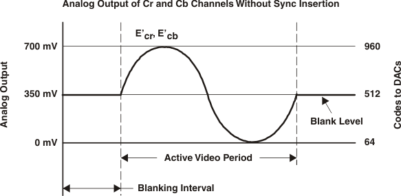 Figure 6-45 Analog Output of Cr and Cb Channels Without Sync Insertion
The blanking level of all channels is at 350 mV. Note that for the Pb and Pr output channels, there is no dc offset added, so DAC input code 0 now corresponds to 0 V dc output. Whether or not offset is added to the DAC outputs is determined from the setting of the dtg2_rgb_mode_on register.
6.8.5 SMPTE-Compatible YPbPr Output With Sync Signal Inserted on All Channels
In this mode, sync signals are inserted on all three channels Y, Cr, and Cb. The Y channel output is identical to that of Section 6.8.4. The Pb and Pr channel outputs are shown below. The range of input codes to the Y channel is from 64 to 940. The range of input codes to the CrCb channels is from 64 to 960.
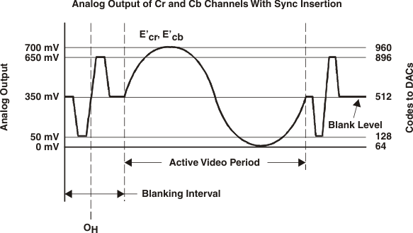 Figure 6-46 Analog Output of Cr and Cb Channels With Sync Insertion
The ac dynamic range during the active video period is the same on all channels, 700 mV. This means that two different code ranges are mapped to the same analog output range. Because three DACs in the THS8200 share a common full-scale adjust resistor, therefore, different input codes to the DAC result in different analog outputs. To map two code ranges into a same analog output, the input code range must be scaled in the CSM block.
6.8.6 Summary of Supported Video Formats
| RGB WITHOUT SYNC | RGB SYNC ON G | RGB SYNC ON ALL |
YPbPr SYNC ON Y | YPbPr SYNC ON ALL | |
|---|---|---|---|---|---|
| Range of input codes | 0 to 1023 | 64 to 940 | 64 to 940 | 64 to 940 on Y; 64 to 960 on Cr and Cb |
64 to 940 on Y; 64 to 960 on Cr and Cb |
| Peak level | 700 mV or 1305 mV | 1050 mV | 1050 mV | 1050 mV | 1050 mV |
| Blank level | 0 V | 350 mV | 350 mV | 350 mV | 350 mV |
| DC level shift during active video period | 0 | 350 mV | 350 mV | 350 mV | 350 mV |
6.9 Test Functions
The user can activate a 75% SMPTE color bar test pattern when the device is configured in VESA mode using the vesa_colorbars register setting. The width of each color bar can be programmed using the dtg1_vesa_cbar_size register.
The digital logic in front of the DACs can be completely bypassed and the DACs can be driven directly with levels programmed from the I2C interface by activating the dac_i2c_cntl register. In this case the dac<n>_cntl registers set the DAC input codes. A fast or slow ramp signal can be internally generated and sent to the DACs using tst_fastramp and tst_slowramp registers. This could be useful for a static DAC linearity test.
Alternatively, the input bus can directly drive the DACs when the tst_digbypass register is activated for tests at full speed.
The delay of the Y channel can be changed in YCbCr modes with respect to Cb and Cr channels by programming the tst_ydelay register.
Finally, there is a digital output port with data encoded according to ITU-R.BT656. This is a loop-through of the original input bus, prior to any THS8200 internal processing, and thus only provides standard data when input to the THS8200 is provided in a 10-bit ITU-R BT.656 format. This output bus could be used to connect to a separate NTSC/PAL video encoder. The data_clk656_on register activates the clock output on this bus and the data_tristate656 register disables the output bus. It is recommended to disable this output when not in use.
6.10 Power Down
THS8200 implements two power-down modes: dac_pwdn powers down the DAC channels but keeps all digital logic active; chip_pwdn powers down the digital logic except the I2C interface. Activating both registers enforces a complete analog/digital power down except for the I2C interface.
6.11 CGMS Insertion
The THS8200 can embed data within the vertical blanking interval, encoded according to the EIA-805 data insertion standard. CGMS is an implementation of the EIA-805 standard that defines data insertion in component video interface (CVI) video signals.
The THS8200 supports CGMS data insertion on line 41 of every frame in the 525P format. The data is inserted on the Y channel only; Pb and Pr channels remain at the blanking level. CGMS data insertion is enabled by activating the cgms_en register and programming the cgms_header and cgms_payload registers appropriately. The user needs to program header and payload data in the correct format, as no additional data encoding is done prior to insertion into the analog DAC output. The THS8200 only performs a play-out function for the programmed data. The CGMS encoding block assumes that a full 10-bit video range is used to determine the 70% of peak-white amplitude of a logic 1 bit, as prescribed by EIA-805. The CSM does not affect the amplitude of the CGMS data insertion.
CGMS is inserted on line 41 as prescribed by EIA 770 standards for progressive format display of SDTV. Fourteen bits can be inserted on this line, consisting of 6 bits header and 8 bits payload. The user can directly program these bits into the corresponding THS8200 registers. Care should be taken to format this data according to CGMS semantics; the user is referred to the original standards to determine header/payload data programming. To avoid the transmission of invalid data, the data transmitted is updated only when the CGMS register with the highest subaddress is programmed with cgms_en active.
CGMS insertion is possible in either 1x or 2x interpolated video modes of the THS8200. While EIA-805 allows the inserted data to change on every frame, and also allows data packets that would span multiple lines (and therefore also multiple frames, since only 1 line/frame is used for insertion), the THS8200 does not support multiline data insertion because it is not required for CGMS.
6.12 I2C Interface
The THS8200 contains a slave-only I2C interface on which both write and read are supported. The register map shows which registers support read/write (R/W) and which are read-only (R). The device supports normal and fast I2C modes (SCL up to 400 kHz). The I2C interface is also operational when no input clock is received on CLKIN.
To discriminate between write and read operations, the device is addressed at separate device addresses. There is an automatic internal sub-address increment counter to efficiently write/read multiple bytes in the register map during one write/read operation. Furthermore, bit1 of the I2C device address is dependent upon the setting of the I2CA pin, as follows:
- If address-selecting pin I2CA = 0, then
- write address is 40h (0100 0000)
- read address is 41h (0100 0001)
- If address-selecting pin I2CA = 1, then
- write address is 42h (0100 0010)
- read address is 43h (0100 0011)
The I2C interface supports fast I2C, that is, SCL up to 400 kHz.
WRITE FORMAT
| S | Slave address(w) | A | Sub-address | A | Data0 | A | ...... | DataN-1 | A | P |
| S | Start condition |
| Slave address(w) | 0100 0000 (0x40) if I2CA = 0, or 0100 0010 (0x42) if I2CA = 1 |
| A | Acknowledge, generated by the THS8200 |
| Sub-address | Sub-address of the first register to write, length: 1 byte |
| Data0 | First byte of the data |
| DataN-1 | Nth byte of the data |
| P | Stop condition |
READ FORMAT
First write the sub-address, where the data must be read out to the THS8200 in the format as follows:
| S | Slave address(w) | A | Sub-address | A | P |
| S | Slave address(r) | A | DataN | AM | Data(N+1) | AM | ...... | NAM | P |
| S | Start condition |
| Slave address(r) | 0100 0001 (0x41) if I2CA = 0, or 0100 0011 (0x43) if I2CA = 1 |
| A | Acknowledge, generated by the THS8200; if the transmission is successful, then A = 0, else A = 1 |
| AM | Acknowledge, generated by a master |
| NAM | Not acknowledge, generated by a master |
| Sub-address | Sub-address of the first register to read, length: 1 byte |
| Data0 | First byte of the data read |
| DataN+1 | Nth byte of the data read |
| P | Stop condition |
In both write and read operations, the sub-address is incremented automatically when multiple bytes are written/read. Therefore, only the first sub-address needs to be supplied to the THS8200.