ZHCS616E March   2012  – February 2017 TCA9554

PRODUCTION DATA.  

  1. 特性
  2. 应用
  3. 说明
    1.     Device Images
      1.      简化框图
  4. 修订历史记录
  5. Pin Configuration and Functions
  6. Specifications
    1. 6.1 Absolute Maximum Ratings
    2. 6.2 ESD Ratings
    3. 6.3 Recommended Operating Conditions
    4. 6.4 Thermal Information
    5. 6.5 Electrical Characteristics
    6. 6.6 I2C Interface Timing Requirements
    7. 6.7 Switching Characteristics
    8. 6.8 Typical Characteristics
  7. Parameter Measurement Information
  8. Detailed Description
    1. 8.1 Overview
    2. 8.2 Functional Block Diagram
    3. 8.3 Feature Description
      1. 8.3.1 I/O Port
      2. 8.3.2 Interrupt Output (INT)
    4. 8.4 Device Functional Modes
      1. 8.4.1 Power-On Reset
    5. 8.5 Programming
      1. 8.5.1 I2C Interface
    6. 8.6 Register Maps
      1. 8.6.1 Device Address
      2. 8.6.2 Control Register and Command Byte
      3. 8.6.3 Register Descriptions
        1. 8.6.3.1 Bus Transactions
          1. 8.6.3.1.1 Writes
          2. 8.6.3.1.2 Reads
  9. Application and Implementation
    1. 9.1 Application Information
    2. 9.2 Typical Application
      1. 9.2.1 Design Requirements
        1. 9.2.1.1 Calculating Junction Temperature and Power Dissipation
        2. 9.2.1.2 Minimizing ICC when I/Os Control LEDs
      2. 9.2.2 Detailed Design Procedure
      3. 9.2.3 Application Curves
  10. 10Power Supply Recommendations
    1. 10.1 Power-On Reset Requirements
  11. 11Layout
    1. 11.1 Layout Guidelines
    2. 11.2 Layout Example
  12. 12器件和文档支持
    1. 12.1 文档支持
      1. 12.1.1 相关文档
    2. 12.2 接收文档更新通知
    3. 12.3 社区资源
    4. 12.4 商标
    5. 12.5 静电放电警告
    6. 12.6 Glossary
  13. 13机械、封装和可订购信息

封装选项

机械数据 (封装 | 引脚)
散热焊盘机械数据 (封装 | 引脚)
订购信息

Reads

The bus master first must send the TCA9554 address with the LSB set to a logic 0 (see Figure 19 for device address). The command byte is sent after the address and determines which register is accessed. After a restart, the device address is sent again but, this time, the LSB is set to a logic 1. Data from the register defined by the command byte then is sent by the TCA9554 (see Figure 25). The command byte does not increment automatically. If multiple bytes are read, data from the specified command byte/register is going to be continuously read.

See the Register Descriptions section for the list of the TCA9554's internal registers and a description of each one.

Figure 24 shows an example of reading a single byte from a slave register.

TCA9554 i2c_read_example.gifFigure 24. Read from Register

After a restart, the value of the register defined by the command byte matches the register being accessed when the restart occurred. Data is clocked into the register on the rising edge of the ACK clock pulse. After the first byte, additional bytes may be read, but the same register specified by the command byte is read.

Data is clocked into the register on the rising edge of the ACK clock pulse. There is no limitation on the number of data bytes received in one read transmission, but when the final byte is received, the bus master must not acknowledge the data.
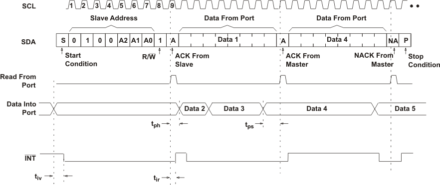
TCA9554 read_input_cps233.gif
Transfer of data can be stopped at any time by a Stop condition. When this occurs, data present at the latest acknowledge phase is valid (output mode). It is assumed that the command byte previously has been set to 00 (Read Input Port register).
This figure eliminates the command byte transfer, a restart, and slave address call between the initial slave address call and actual data transfer from the P port (see Figure 24 for these details).
Figure 25. Read Input Port Register