ZHCSAT1D December   2012  – July 2017 TCA9517

PRODUCTION DATA.  

  1. 特性
  2. 应用
  3. 说明
    1.     Device Images
      1.      简化的原理图
  4. 修订历史记录
  5. 说明 (续)
  6. Pin Configuration and Functions
    1.     Pin Functions
  7. Specifications
    1. 7.1 Absolute Maximum Ratings
    2. 7.2 ESD Ratings
    3. 7.3 Recommended Operating Conditions
    4. 7.4 Thermal Information
    5. 7.5 Electrical Characteristics
    6. 7.6 Timing Requirements
    7. 7.7 I2C Interface Switching Characteristics
    8. 7.8 Typical Characteristics
  8. Parameter Measurement Information
  9. Detailed Description
    1. 9.1 Overview
    2. 9.2 Functional Block Diagram
    3. 9.3 Feature Description
      1. 9.3.1 Two-Channel Bidirectional Buffer
      2. 9.3.2 Active-High Repeater-Enable Input
      3. 9.3.3 VOL B-Side Offset Voltage
      4. 9.3.4 Standard Mode and Fast Mode Support
      5. 9.3.5 Clock Stretching Support
    4. 9.4 Device Functional Modes
  10. 10Application and Implementation
    1. 10.1 Application Information
    2. 10.2 Typical Application
      1. 10.2.1 Design Requirements
      2. 10.2.2 Detailed Design Procedure
        1. 10.2.2.1 Clock Stretching Support
        2. 10.2.2.2 VILC and Pullup Resistor Sizing
      3. 10.2.3 Application Curve
  11. 11Power Supply Recommendations
  12. 12Layout
    1. 12.1 Layout Guidelines
    2. 12.2 Layout Example
  13. 13器件和文档支持
    1. 13.1 社区资源
    2. 13.2 商标
    3. 13.3 静电放电警告
    4. 13.4 Glossary
  14. 14机械、封装和可订购信息

封装选项

机械数据 (封装 | 引脚)
散热焊盘机械数据 (封装 | 引脚)
订购信息

Pin Configuration and Functions

D Packages
8-Pin SOIC
Top View
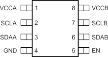
TCA9517 po_cps245_2.gif
DGK Package
8-Pin VSSOP
Top View
TCA9517 po_cps245.gif

Pin Functions

PINTYPEDESCRIPTION
NO.NAME
1 VCCA Supply A-side supply voltage (0.9 V to 5.5 V)
2 SCLA Input/Output Serial clock bus, A-side. Connect to VCCA through a pull-up resistor. If unused, connect directly to ground.
3 SDAA Input/Output Serial data bus, A-side. Connect to VCCA through a pull-up resistor. If unused, connect directly to ground.
4 GND Ground Ground
5 EN Input Active-high repeater enable input
6 SDAB Input/Output Serial data bus, B-side. Connect to VCCB through a pull-up resistor. If unused, connect directly to ground.
7 SCLB Input/Output Serial clock bus, B-side. Connect to VCCB through a pull-up resistor. If unused, connect directly to ground.
8 VCCB Supply B-side and device supply voltage (2.7 V to 5.5 V)