ZHCSFH3A September   2016  – February 2023 TCA6408A-Q1

PRODUCTION DATA  

  1. 特性
  2. 应用
  3. 说明
  4. Revision History
  5. Pin Configuration and Functions
  6. Specifications
    1. 6.1 Absolute Maximum Ratings
    2. 6.2 ESD Ratings
    3. 6.3 Recommended Operating Conditions
    4. 6.4 Thermal Information
    5. 6.5 Electrical Characteristics
    6. 6.6 I2C Interface Timing Requirements
    7. 6.7 Reset Timing Requirements
    8. 6.8 Switching Characteristics
    9. 6.9 Typical Characteristics
  7. Parameter Measurement Information
  8. Detailed Description
    1. 8.1 Overview
    2. 8.2 Functional Block Diagrams
    3. 8.3 Feature Description
      1. 8.3.1 Voltage Translation
      2. 8.3.2 I/O Port
      3. 8.3.3 Interrupt Output ( INT)
      4. 8.3.4 Reset Input ( RESET)
    4. 8.4 Device Functional Modes
      1. 8.4.1 Power-On Reset (POR)
      2. 8.4.2 Powered-Up
    5. 8.5 Programming
      1. 8.5.1 I2C Interface
      2. 8.5.2 Bus Transactions
        1. 8.5.2.1 Writes
        2. 8.5.2.2 Reads
    6. 8.6 Register Map
      1. 8.6.1 Device Address
      2. 8.6.2 Control Register and Command Byte
      3. 8.6.3 Register Descriptions
  9. Application and Implementation
    1. 9.1 Application Information
    2. 9.2 Typical Application
      1. 9.2.1 Design Requirements
        1. 9.2.1.1 Calculating Junction Temperature and Power Dissipation
        2. 9.2.1.2 Minimizing ICC When I/O is Used to Control LEDs
      2. 9.2.2 Detailed Design Procedure
      3. 9.2.3 Application Curves
    3. 9.3 Power Supply Recommendations
      1. 9.3.1 Power-On Reset Requirements
    4. 9.4 Layout
      1. 9.4.1 Layout Guidelines
      2. 9.4.2 Layout Example
  10. 10Device and Documentation Support
    1. 10.1 Receiving Notification of Documentation Updates
    2. 10.2 商标
    3. 10.3 静电放电警告
    4. 10.4 术语表
  11. 11支持资源
  12. 12Mechanical, Packaging, and Orderable Information

封装选项

机械数据 (封装 | 引脚)
散热焊盘机械数据 (封装 | 引脚)
订购信息

Minimizing ICC When I/O is Used to Control LEDs

When the I/Os are used to control LEDs, normally they are connected to VCC through a resistor as shown in GUID-4D38174B-449A-4391-9732-FEAC63A5C0EF.html#SCPS2348238. The LED acts as a diode, so when the LED is off, the I/O VIN is about 1.2 V less than VCC. The ΔICC parameter in the GUID-C28FBBDC-9725-4E28-82C3-3AC80EAD8B8D.html#GUID-C28FBBDC-9725-4E28-82C3-3AC80EAD8B8D table shows how ICC increases as VIN becomes lower than VCC. Designs that must minimize current consumption, such as battery power applications, must consider maintaining the I/O pins greater than or equal to VCC when the LED is off.

#SCPS2343321 shows a high-value resistor in parallel with the LED. #SCPS2341867 shows VCC less than the LED supply voltage by at least 1.2 V. Both of these methods maintain the I/O VIN at or above VCC and prevent additional supply current consumption when the LED is off.
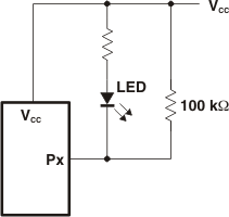
GUID-D72972DA-9AD5-4BFA-93DC-7FFDD3A38A0F-low.gifFigure 9-2 High-Value Resistor in Parallel With LED
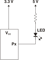
GUID-46B3CF57-15B0-4234-96B6-934A4CF103BD-low.gifFigure 9-3 Device Supplied by a Low Voltage