ZHCSHK8E october 2017 – july 2023 TAS2770
PRODUCTION DATA
- 1
- 1 特性
- 2 应用
- 3 说明
- 4 Revision History
- 5 Pin Configuration and Functions
- 6 Specifications
- 7 Parameter Measurement Information
-
8 Detailed Description
- 8.1 Overview
- 8.2 Functional Block Diagram
- 8.3 Feature Description
- 8.4 Device Functional Modes
- 8.5
Register Maps
- 8.5.1 Register Summary Table Book=0x00 Page=0x00
- 8.5.2
Register Maps
- 8.5.2.1 PAGE (book=0x00 page=0x00 address=0x00) [reset=0h]
- 8.5.2.2 SW_RESET (book=0x00 page=0x00 address=0x01) [reset=0h]
- 8.5.2.3 PWR_CTL (book=0x00 page=0x00 address=0x02) [reset=Eh]
- 8.5.2.4 PB_CFG0 (book=0x00 page=0x00 address=0x03) [reset=10h]
- 8.5.2.5 PB_CFG1 (book=0x00 page=0x00 address=0x04) [reset=1h]
- 8.5.2.6 PB_CFG2 (book=0x00 page=0x00 address=0x05) [reset=0h]
- 8.5.2.7 PB_CFG3 (book=0x00 page=0x00 address=0x06) [reset=0h]
- 8.5.2.8 MISC_CFG (book=0x00 page=0x00 address=0x07) [reset=6h]
- 8.5.2.9 PDM_CFG0 (book=0x00 page=0x00 address=0x08) [reset=0h]
- 8.5.2.10 PDM_CFG1 (book=0x00 page=0x00 address=0x09) [reset=8h]
- 8.5.2.11 TDM_CFG0 (book=0x00 page=0x00 address=0x0A) [reset=7h]
- 8.5.2.12 TDM_CFG1 (book=0x00 page=0x00 address=0x0B) [reset=2h]
- 8.5.2.13 TDM_CFG2 (book=0x00 page=0x00 address=0x0C) [reset=Ah]
- 8.5.2.14 TDM_CFG3 (book=0x00 page=0x00 address=0x0D) [reset=10h]
- 8.5.2.15 TDM_CFG4 (book=0x00 page=0x00 address=0x0E) [reset=13h]
- 8.5.2.16 TDM_CFG5 (book=0x00 page=0x00 address=0x0F) [reset=2h]
- 8.5.2.17 TDM_CFG6 (book=0x00 page=0x00 address=0x10) [reset=0h]
- 8.5.2.18 TDM_CFG7 (book=0x00 page=0x00 address=0x11) [reset=4h]
- 8.5.2.19 TDM_CFG8 (book=0x00 page=0x00 address=0x12) [reset=6h]
- 8.5.2.20 TDM_CFG9 (book=0x00 page=0x00 address=0x13) [reset=7h]
- 8.5.2.21 TDM_CFG10 (book=0x00 page=0x00 address=0x14) [reset=8h]
- 8.5.2.22 LIM_CFG0 (book=0x00 page=0x00 address=0x15) [reset=14h]
- 8.5.2.23 LIM_CFG1 (book=0x00 page=0x00 address=0x16) [reset=76h]
- 8.5.2.24 LIM_CFG2 (book=0x00 page=0x00 address=0x17) [reset=10h]
- 8.5.2.25 LIM_CFG3 (book=0x00 page=0x00 address=0x18) [reset=6Eh]
- 8.5.2.26 LIM_CFG4 (book=0x00 page=0x00 address=0x19) [reset=1Eh]
- 8.5.2.27 LIM_CFG5 (book=0x00 page=0x00 address=0x1A) [reset=58h]
- 8.5.2.28 BOP_CFG0 (book=0x00 page=0x00 address=0x1B) [reset=1h]
- 8.5.2.29 BOP_CFG1 (book=0x00 page=0x00 address=0x1C) [reset=14h]
- 8.5.2.30 BOP_CFG2 (book=0x00 page=0x00 address=0x1D) [reset=4Eh]
- 8.5.2.31 ICLA_CFG0 (book=0x00 page=0x00 address=0x1E) [reset=0h]
- 8.5.2.32 ICLA_CFG1 (book=0x00 page=0x00 address=0x1F) [reset=0h]
- 8.5.2.33 INT_MASK0 (book=0x00 page=0x00 address=0x20) [reset=FCh]
- 8.5.2.34 INT_MASK1 (book=0x00 page=0x00 address=0x21) [reset=B1h]
- 8.5.2.35 INT_LIVE0 (book=0x00 page=0x00 address=0x22) [reset=0h]
- 8.5.2.36 INT_LIVE1 (book=0x00 page=0x00 address=0x23) [reset=0h]
- 8.5.2.37 INT_LTCH0 (book=0x00 page=0x00 address=0x24) [reset=0h]
- 8.5.2.38 INT_LTCH1 (book=0x00 page=0x00 address=0x25) [reset=0h]
- 8.5.2.39 INT_LTCH2 (book=0x00 page=0x00 address=0x26) [reset=0h]
- 8.5.2.40 VBAT_MSB (book=0x00 page=0x00 address=0x27) [reset=0h]
- 8.5.2.41 VBAT_LSB (book=0x00 page=0x00 address=0x28) [reset=0h]
- 8.5.2.42 TEMP_MSB (book=0x00 page=0x00 address=0x29) [reset=0h]
- 8.5.2.43 TEMP_LSB (book=0x00 page=0x00 address=0x2A) [reset=0h]
- 8.5.2.44 INT_CFG (book=0x00 page=0x00 address=0x30) [reset=5h]
- 8.5.2.45 DIN_PD (book=0x00 page=0x00 address=0x31) [reset=0h]
- 8.5.2.46 MISC_IRQ (book=0x00 page=0x00 address=0x32) [reset=81h]
- 8.5.2.47 CLOCK_CFG (book=0x00 page=0x00 address=0x3C) [reset=Dh]
- 8.5.2.48 TDM_DET (book=0x00 page=0x00 address=0x77) [reset=7Fh]
- 8.5.2.49 REV_ID (book=0x00 page=0x00 address=0x7D) [reset=20h]
- 8.5.2.50 I2C_CKSUM (book=0x00 page=0x00 address=0x7E) [reset=0h]
- 8.5.2.51 BOOK (book=0x00 page=0x00 address=0x7F) [reset=0h]
-
9 Application and Implementation
- 9.1 Application Information
- 9.2 Typical Application
- 9.3
Initialization Set Up
- 9.3.1 Initial Device Configuration - Auto Rate
- 9.3.2 Initial Device Configuration - 48 kHz
- 9.3.3 Initial Device Configuration - 44.1 kHz
- 9.3.4 Sample Rate Change - 48 kHz to 44.1kHz
- 9.3.5 Sample Rate Change - 44.1 kHz to 48 kHz
- 9.3.6 Device Mute
- 9.3.7 Device Un-Mute
- 9.3.8 Device Sleep
- 9.3.9 Device Wake
- 10Power Supply Recommendations
- 11Layout
- 12Device and Documentation Support
- 13Mechanical, Packaging, and Orderable Information
8.4.1 PDM Input
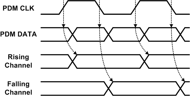
The TAS2770 provides one PDM input that can be used for low latency audio playback or sensor aggregation in TDM/I2C mode. Figure 8-6 below illustrates the double data rate nature of the PDM inputs. Each input has two interleaved PDM channels, one sampled by the rising edge and the other by the falling edge of the clock.
 Figure 8-6 PDM Waveform
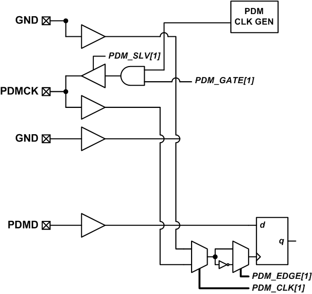
The PDM inputs are sampled by the PDMCK pin, which can be independently configured as either a PDM clock slave input or a PDM clock master output. The PDM_EDGE[1:0] and PDM_SLV[1:0] register bits select the sample clock edge and master/slave mode for each of the two PDM inputs. In master mode the PDMCK pin can disable the clocks (and drive a logic 0) by setting the PDM_GATE[1:0] register bits low. The PDM_CLK[1:0] register bits select which clock is used to sample each PDM input.
 Figure 8-7 PDM Data and Clock Input Block Diagram
When configured as a clock slave, the PDM clock input does not require a specific phase relationship to the system clock (SBCLK in TDM/I2C Mode), but must have an exact frequency relationship to the audio sample rate. This is equivalent to 64/32/16 (~3 MHz) or 128/64/32 (~6 MHz) times a single/double/quadruple speed sample rate. The PDM rate is set by the PDM_RATE1[1:0] register bits.
When the PDMCK pin is configured as a clock master, the TAS2770 will output a 50% duty cycle clock of frequency that is set by the PDM_RATE1[1:0] register bits (64/32/16 or 128/64/32 times a single/double/quadruple speed sample rate).
The PDM_MAP register bit selects which PDM pin is used for audio playback input and which is used for PDM sensor input. The PDM sensor input can be decimated (time aligned with the IV sense) and transmitted on the SDOUT pin when the device is in TDM/I2C mode.
| PDM Input Pin | Register Bit | Value | Capture Edge |
|---|---|---|---|
| PDMD | PDM_EDGE[1] | | Rising (default) |
| Falling |
| PDM Input Pin | Register Bit | Value | Master/Slave |
|---|---|---|---|
| PDMD | PDM_SLV[1] | | Slave (default) |
| Master |
| PDM Input Pin | Register Bit | Value | Clock Source |
|---|---|---|---|
| PDMD | PDM_CLK[1] | | GND |
| PDMCK (default) |
| PDM Clock Pin | Register Bit | Value | Gating |
|---|---|---|---|
| PDMCK | PDM_GATE[1] | | Gated Off (default) |
| Active |
| PDM Input Pin | Register Bits | Value | Sample Rate |
|---|---|---|---|
| PDMD | PDM_RATE1[1:0] | | 2.54 - 3.38 MHz (default) |
| 5.08 - 6.76 MHz | ||
| Reserved | ||
| Reserved |
| PDM_MAP | Mapping |
|---|---|
| PDMD pin for sensor input (default) |
| PDMD pin for playback |