SLLS259J November 1996 – October 2016 SN75LVDS82
PRODUCTION DATA.
- 1 Features
- 2 Applications
- 3 Description
- 4 Revision History
- 5 Description (continued)
- 6 Pin Configuration and Functions
- 7 Specifications
- 8 Parameter Measurement Information
- 9 Detailed Description
- 10Application and Implementation
- 11Power Supply Recommendations
- 12Layout
- 13Device and Documentation Support
- 14Mechanical, Packaging, and Orderable Information
9 Detailed Description
9.1 Overview
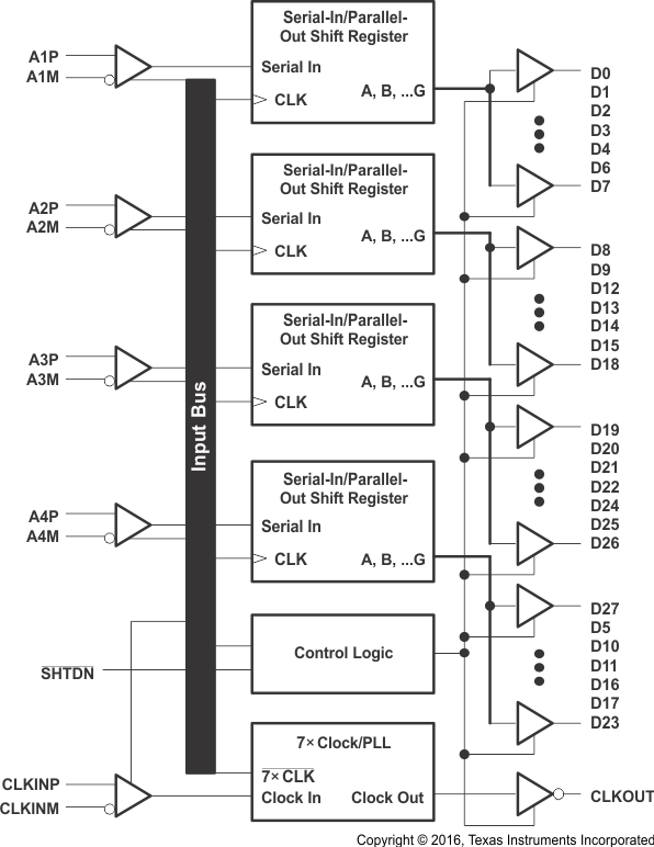
The SN75LVDS82 implements five low-voltage differential signal (LVDS) line receivers: 4 data lanes and 1 clock lane. The clock is internally multiplied by 7 and used for sampling LVDS data. Each input lane contains a shift register that converts serial data to parallel. 28 total bits per clock period are deserialized and presented on the LVTTL output bus
9.2 Functional Block Diagram

9.3 Feature Description
9.3.1 LVDS Input Data
The SN65LVDS82 is a simple deserializer that ignores bit representation in the LVDS stream. The data inputs to the receiver come from a transmitters such as the SN75LVDS83B and consist of up to 24 bits of video information, a horizontal synchronization bit, a vertical synchronization bit, an enable bit, and a spare bit.
The pixel data assignment is listed in Table 1 for 24-bit, 18-bit, and 12-bit color hosts.
Table 1. Pixel Data Assignment
| SERIAL CHANNEL | DATA BITS | 8-BIT | 6-BIT | 4-BIT | |||
|---|---|---|---|---|---|---|---|
| FORMAT-1 | FORMAT-2 | FORMAT-3 | NON-LINEAR STEP SIZE | LINEAR STEP SIZE | |||
| Y0 | D0 | R0D27 | R2 | R2 | R0 | R2 | VCC |
| D1 | R1 | R3 | R3 | R1 | R3 | GND | |
| D2 | R2 | R4 | R4 | R2 | R0 | R0 | |
| D3 | R3 | R5 | R5 | R3 | R1 | R1 | |
| D4 | R4 | R6 | R6 | R4 | R2 | R2 | |
| D6 | R5 | R7 | R7 | R5 | R3 | R3 | |
| D7 | G0 | G2 | G2 | G0 | G2 | VCC | |
| Y1 | D8 | G1 | G3 | G3 | G1 | G3 | GND |
| D9 | G2 | G4 | G4 | G2 | G0 | G0 | |
| D12 | G3 | G5 | G5 | G3 | G1 | G1 | |
| D13 | G4 | G6 | G6 | G4 | G2 | G2 | |
| D14 | G5 | G7 | G7 | G5 | G3 | G3 | |
| D15 | B0 | B2 | B2 | B0 | B2 | VCC | |
| D18 | B1 | B3 | B3 | B1 | B3 | GND | |
| Y2 | D19 | B2 | B4 | B4 | B2 | B0 | B0 |
| D20 | B3 | B5 | B5 | B3 | B1 | B1 | |
| D21 | B4 | B6 | B6 | B4 | B2 | B2 | |
| D22 | B5 | B7 | B7 | B5 | B3 | B3 | |
| D24 | HSYNC | HSYNC | HSYNC | HSYNC | HSYNC | HSYNC | |
| D25 | VSYNC | VSYNC | VSYNC | VSYNC | VSYNC | VSYNC | |
| D26 | ENABLE | ENABLE | ENABLE | ENABLE | ENABLE | ENABLE | |
| Y3 | D27 | R6 | R0 | GND | GND | GND | GND |
| D5 | R7 | R1 | GND | GND | GND | GND | |
| D10 | G6 | G0 | GND | GND | GND | GND | |
| D11 | G7 | G1 | GND | GND | GND | GND | |
| D16 | B6 | B0 | GND | GND | GND | GND | |
| D17 | B7 | B1 | GND | GND | GND | GND | |
| D23 | RSVD | RSVD | GND | GND | GND | GND | |
| CLKOUT | CLKIN | CLK | CLK | CLK | CLK | CLK | CLK |
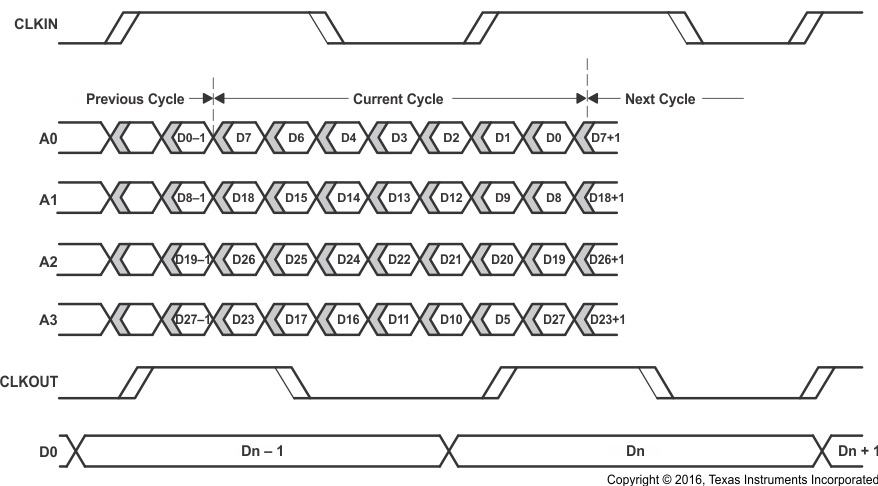
 Figure 12. SN75LVDS82 Load and Shift Timing Sequences
9.4 Device Functional Modes
9.4.1 Low Power Mode
The SN75LVDS82 can be put in low-power consumption mode by active-low input SHTDN. Connecting pin SHTDN to GND inhibits the clock and shut off the LVDS output drivers for lower power consumption. A low level on this signal clears all internal registers to a low-level. Populate a pull-up to VCC on SHTDN to enable the device for normal operation.
9.4.2 Test Patterns
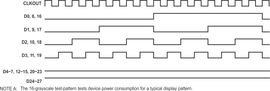
 Figure 13. 16-Grayscale Test-Pattern Waveforms
 Figure 14. Worst-Case Test-Pattern Waveforms

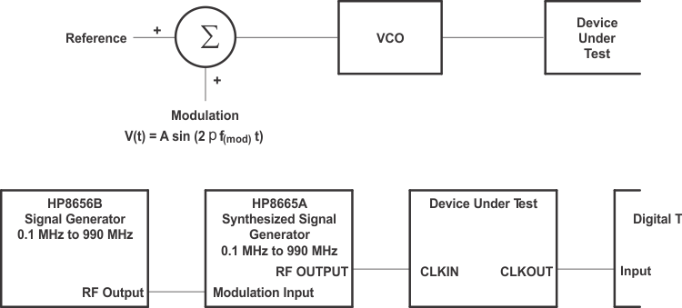
 Figure 15. Input Clock Jitter Test