SCAS218X January 1993 – January 2015 SN74LVC245A
PRODUCTION DATA.
- 1 Features
- 2 Applications
- 3 Simplified Schematic
- 4 Revision History
- 5 Pin Configuration and Functions
- 6 Specifications
- 7 Parameter Measurement Information
- 8 Detailed Description
- 9 Application and Implementation
- 10Power Supply Recommendations
- 11Layout
- 12Device and Documentation Support
- 13Mechanical, Packaging, and Orderable Information
封装选项
请参考 PDF 数据表获取器件具体的封装图。
机械数据 (封装 | 引脚)
- DGV|20
- DB|20
- NS|20
- N|20
- DW|20
- PW|20
- RGY|20
散热焊盘机械数据 (封装 | 引脚)
- RGY|20
订购信息
6 Specifications
6.1 Absolute Maximum Ratings
over operating free-air temperature range (unless otherwise noted)(1)| MIN | MAX | UNIT | |||
|---|---|---|---|---|---|
| VCC | Supply voltage range | –0.5 | 6.5 | V | |
| VI | Input voltage range(2) | –0.5 | 6.5 | V | |
| VO | Voltage range applied to any output in the high-impedance or power-off state(2) | –0.5 | 6.5 | V | |
| VO | Voltage range applied to any output in the high or low state(2)(3) | –0.5 | VCC + 0.5 | V | |
| IIK | Input clamp current | VI < 0 | –50 | mA | |
| IOK | Output clamp current | VO < 0 | –50 | mA | |
| IO | Continuous output current | ±50 | mA | ||
| Continuous current through VCC or GND | ±100 | mA | |||
| Tstg | Storage temperature range | –65 | 150 | °C | |
(1) Stresses beyond those listed under Absolute Maximum Ratings may cause permanent damage to the device. These are stress ratings only, and functional operation of the device at these or any other conditions beyond those indicated under Recommended Operating Conditions is not implied. Exposure to absolute-maximum-rated conditions for extended periods may affect device reliability.
(2) The input and output negative-voltage ratings may be exceeded if the input and output current ratings are observed.
(3) The value of VCC is provided in the Recommended Operating Conditions table.
6.2 ESD Ratings
| PARAMETER | DEFINITION | VALUE | UNIT | |
|---|---|---|---|---|
| V(ESD) | Electrostatic discharge | Human body model (HBM), per ANSI/ESDA/JEDEC JS-001, all pins(1) | 2000 | V |
| Charged device model (CDM), per JEDEC specification JESD22-C101, all pins(2) | 1000 | |||
(1) JEDEC document JEP155 states that 500-V HBM allows safe manufacturing with a standard ESD control process.
(2) JEDEC document JEP157 states that 250-V CDM allows safe manufacturing with a standard ESD control process.
Recommended Operating Conditions
over operating free-air temperature range (unless otherwise noted)(1)| TA = 25°C | –40°C TO 85°C | –40°C TO 125°C | UNIT | ||||||
|---|---|---|---|---|---|---|---|---|---|
| MIN | MAX | MIN | MAX | MIN | MAX | ||||
| VCC | Supply voltage | Operating | 1.65 | 3.6 | 1.65 | 3.6 | 1.65 | 3.6 | V |
| Data retention only | 1.5 | 1.5 | 1.5 | ||||||
| VIH | High-level input voltage | VCC = 1.65 V to 1.95 V | 0.65 × VCC | 0.65 × VCC | 0.65 × VCC | V | |||
| VCC = 2.3 V to 2.7 V | 1.7 | 1.7 | 1.7 | ||||||
| VCC = 2.7 V to 3.6 V | 2 | 2 | 2 | ||||||
| VIL | Low-level input voltage | VCC = 1.65 V to 1.95 V | 0.35 × VCC | 0.35 × VCC | 0.35 × VCC | V | |||
| VCC = 2.3 V to 2.7 V | 0.7 | 0.7 | 0.7 | ||||||
| VCC = 2.7 V to 3.6 V | 0.8 | 0.8 | 0.8 | ||||||
| VI | Input voltage | 0 | 5.5 | 0 | 5.5 | 0 | 5.5 | V | |
| VO | Output voltage | 0 | VCC | 0 | VCC | 0 | VCC | V | |
| IOH | High-level output current | VCC = 1.65 V | –4 | –4 | –4 | mA | |||
| VCC = 2.3 V | –8 | –8 | –8 | ||||||
| VCC = 2.7 V | –12 | –12 | –12 | ||||||
| VCC = 3 V | –24 | –24 | –24 | ||||||
| IOL | Low-level output current | VCC = 1.65 V | 4 | 4 | 4 | mA | |||
| VCC = 2.3 V | 8 | 8 | 8 | ||||||
| VCC = 2.7 V | 12 | 12 | 12 | ||||||
| VCC = 3 V | 24 | 24 | 24 | ||||||
| Δt/Δv | Input transition rise or fall rate | 10 | 10 | 10 | ns/V | ||||
(1) All unused inputs of the device must be held at VCC or GND to ensure proper device operation. Refer to the TI application report, Implications of Slow or Floating CMOS Inputs, literature number SCBA004.
6.3 Thermal Information
| THERMAL METRIC(1) | SN74LVC245A | UNIT | ||||||||
|---|---|---|---|---|---|---|---|---|---|---|
| DB(2) | DGV(2) | DW(2) | GQN or ZQN(2) | N(2) | NS(2) | PW(2) | RGY(3) | |||
| 20 PINS | ||||||||||
| RθJA | Junction-to-ambient thermal resistance | 106.5 | 124.1 | 92.9 | 78 | 59.2 | 83.6 | 108.1 | 44.0 | °C/W |
| RθJC(top) | Junction-to-case(top) thermal resistance | 68.1 | 39.5 | 60.6 | 44.9 | 49.4 | 43.0 | 53.0 | ||
| RθJB | Junction-to-board thermal resistance | 61.7 | 65.5 | 60.4 | 40.1 | 51.2 | 59.1 | 22.1 | ||
| ψJT | Junction-to-top characterization parameter | 28.5 | 2.1 | 28.2 | 29.9 | 21.9 | 4.7 | 3.0 | ||
| ψJB | Junction-to-board characterization parameter | 61.2 | 64.9 | 60.0 | 39.9 | 50.8 | 58.6 | 22.2 | ||
| RθJC(bot) | Junction-to-case(bottom) thermal resistance | — | — | — | — | — | — | 16.6 | ||
(1) For more information about traditional and new thermal metrics, see the IC Package Thermal Metrics application report, SPRA953.
(2) The package thermal impedance is calculated in accordance with JESD 51-7.
(3) The package thermal impedance is calculated in accordance with JESD 51-5.
Electrical Characteristics
over recommended operating free-air temperature range (unless otherwise noted)| PARAMETER | TEST CONDITIONS | VCC | TA = 25°C | –40°C TO 85°C | –40°C TO 125°C | UNIT | ||||||
|---|---|---|---|---|---|---|---|---|---|---|---|---|
| MIN | TYP | MAX | MIN | MAX | MIN | MAX | ||||||
| VOH | IOH = –100 μA | 1.65 V to 3.6 V |
VCC – 0.2 | VCC – 0.2 | VCC – 0.2 | V | ||||||
| IOH = –4 mA | 1.65 V | 1.29 | 1.2 | 1.1 | ||||||||
| IOH = –8 mA | 2.3 V | 1.9 | 1.7 | 1.6 | ||||||||
| IOH = –12 mA | 2.7 V | 2.2 | 2.2 | 2.1 | ||||||||
| 3 V | 2.4 | 2.4 | 2.3 | |||||||||
| IOH = –24 mA | 3 V | 2.3 | 2.2 | 2.1 | ||||||||
| VOL | IOL = 100 μA | 1.65 V to 3.6 V |
0.1 | 0.2 | 0.2 | V | ||||||
| IOL = 4 mA | 1.65 V | 0.24 | 0.45 | 0.60 | ||||||||
| IOL = 8 mA | 2.3 V | 0.3 | 0.7 | 0.75 | ||||||||
| IOL = 12 mA | 2.7 V | 0.4 | 0.4 | 0.6 | ||||||||
| IOL = 24 mA | 3 V | 0.55 | 0.55 | 0.75 | ||||||||
| II | Control inputs |
VI = 0 to 5.5 V | 3.6 V | ±1 | ±5 | ±10 | μA | |||||
| Ioff | VI or VO = 5.5 V | 0 | ±1 | ±10 | ±20 | μA | ||||||
| IOZ(1) | VO = 0 to 5.5 V | 3.6 V | ±1 | ±10 | ±20 | μA | ||||||
| ICC | VI = VCC or GND | IO = 0 | 3.6 V | 1 | 10 | 30 | μA | |||||
| 3.6 V ≤ VI ≤ 5.5 V(2) | 1 | 10 | 30 | |||||||||
| ΔICC | One input at VCC – 0.6 V, Other inputs at VCC or GND |
2.7 V to 3.6 V |
500 | 500 | 5000 | μA | ||||||
| Ci | Control inputs | VI = VCC or GND | 3.3 V | 4 | pF | |||||||
| Cio | A or B ports(3) | VI = VCC or GND | 3.3 V | 5.5 | pF | |||||||
(1) All typical values are at VCC = 3.3 V, TA = 25 C.
(2) This applies in the disabled state only.
(3) For I/O ports, the parameter Ioz includes the input leakage current.
Switching Characteristics
over recommended operating free-air temperature range (unless otherwise noted) (see Figure 3)| PARAMETER | FROM (INPUT) |
TO (OUTPUT) |
VCC | TA = 25°C | –40°C TO 85°C | –40°C TO 125°C | UNIT | ||||
|---|---|---|---|---|---|---|---|---|---|---|---|
| MIN | TYP | MAX | MIN | MAX | MIN | MAX | |||||
| tpd | A or B | B or A | 1.8 V ± 0.15 V | 1 | 6 | 12.2 | 1 | 12.7 | 1 | 13.7 | ns |
| 2.5 V ± 0.2 V | 1 | 3.9 | 7.8 | 1 | 8.3 | 1 | 9.1 | ||||
| 2.7 V | 1 | 4.2 | 7.1 | 1 | 7.3 | 1 | 8.3 | ||||
| 3.3 V ± 0.3 V | 1.5 | 3.8 | 6.1 | 1.5 | 6.3 | 1.5 | 7.3 | ||||
| ten | OE | A or B | 1.8 V ± 0.15 V | 1 | 7 | 14.8 | 1 | 15.3 | 1 | 16.8 | ns |
| 2.5 V ± 0.2 V | 1 | 4.5 | 10 | 1 | 10.5 | 1 | 12 | ||||
| 2.7 V | 1 | 5.4 | 9.3 | 1 | 9.5 | 1 | 11 | ||||
| 3.3 V ± 0.3 V | 1.5 | 4.4 | 8.3 | 1.5 | 8.5 | 1.5 | 10 | ||||
| tdis | OE | A or B | 1.8 V ± 0.15 V | 1 | 7.8 | 16.5 | 1 | 17 | 1 | 18 | ns |
| 2.5 V ± 0.2 V | 1 | 4 | 9 | 1 | 9.5 | 1 | 10.5 | ||||
| 2.7 V | 1 | 4.4 | 8.3 | 1 | 8.5 | 1 | 9.5 | ||||
| 3.3 V ± 0.3 V | 1.7 | 4.1 | 7.3 | 1.7 | 7.5 | 1.7 | 8.5 | ||||
| tsk(o) | 3.3 V ± 0.3 V | 1 | 1.5 | ns | |||||||
Operating Characteristics
TA = 25°C| PARAMETER | TEST CONDITIONS |
VCC | TYP | UNIT | ||
|---|---|---|---|---|---|---|
| Cpd | Power dissipation capacitance per transceiver | Outputs enabled | f = 10 MHz | 1.8 V | 42 | pF |
| 2.5 V | 43 | |||||
| 3.3 V | 45 | |||||
| Outputs disabled | 1.8 V | 1 | ||||
| 2.5 V | 1 | |||||
| 3.3 V | 2 | |||||
6.4 Typical Characteristics
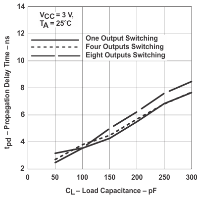 Figure 1. Propagation Delay (Low to High Transition)
vs Load Capacitance
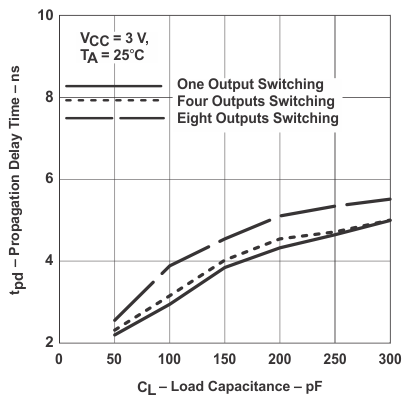 Figure 2. Propagation Delay (High to Low Transition)
vs Load Capacitance