SCAS218X January 1993 – January 2015 SN74LVC245A
PRODUCTION DATA.
- 1 Features
- 2 Applications
- 3 Simplified Schematic
- 4 Revision History
- 5 Pin Configuration and Functions
- 6 Specifications
- 7 Parameter Measurement Information
- 8 Detailed Description
- 9 Application and Implementation
- 10Power Supply Recommendations
- 11Layout
- 12Device and Documentation Support
- 13Mechanical, Packaging, and Orderable Information
封装选项
请参考 PDF 数据表获取器件具体的封装图。
机械数据 (封装 | 引脚)
- DGV|20
- DB|20
- NS|20
- N|20
- DW|20
- PW|20
- RGY|20
散热焊盘机械数据 (封装 | 引脚)
- RGY|20
订购信息
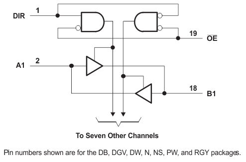
8 Detailed Description
8.1 Overview
This octal bus transceiver is designed for 1.65-V to 3.6-V VCC operation.
The SN74LVC245A device is designed for asynchronous communication between data buses. This device transmits data from the A bus to the B bus or from the B bus to the A bus, depending on the logic level at the direction-control (DIR) input. The output-enable (OE) input can be used to disable the device so the buses effectively are isolated.
To ensure the high-impedance state during power up or power down, OE should be tied to VCC through a pull-up resistor; the minimum value of the resistor is determined by the current-sinking capability of the driver.
Inputs can be driven from either 3.3-V or 5-V devices. This feature allows the use of this device as a translator in a mixed 3.3-V/5-V system environment.
This device is fully specified for partial-power-down applications using Ioff. The Ioff circuitry disables the outputs, preventing damaging current backflow through the device when it is powered down.
8.2 Functional Block Diagram
8.3 Feature Description
- Allows down voltage translation
- 5 V to 3.3 V
- 5 V or 3.3 V to 1.8 V
- Inputs accept voltage levels up to 5.5 V
8.4 Device Functional Modes
Table 1. Function Table
| INPUTS | OPERATION | |
|---|---|---|
| OE | DIR | |
| L | L | B data to A bus |
| L | H | A data to B bus |
| H | X | Isolation |