SCES414P November 2002 – November 2016 SN74LVC1G57
PRODUCTION DATA.
- 1 Features
- 2 Applications
- 3 Description
- 4 Revision History
- 5 Pin Configuration and Functions
- 6 Specifications
- 7 Parameter Measurement Information
- 8 Detailed Description
- 9 Application and Implementation
- 10Power Supply Recommendations
- 11Layout
- 12Device and Documentation Support
- 13Mechanical, Packaging, and Orderable Information
封装选项
机械数据 (封装 | 引脚)
散热焊盘机械数据 (封装 | 引脚)
- DRY|6
订购信息
9 Application and Implementation
NOTE
Information in the following applications sections is not part of the TI component specification, and TI does not warrant its accuracy or completeness. TI’s customers are responsible for determining suitability of components for their purposes. Customers should validate and test their design implementation to confirm system functionality.
9.1 Application Information
The SN74LVC1G57 features configurable multiple functions. The output state is determined by eight patterns of 3-bit input. The user can choose the logic functions AND, NAND, NOR, XNOR, inverter, and buffer. All inputs can be connected to VCC or GND.
9.2 Typical Application
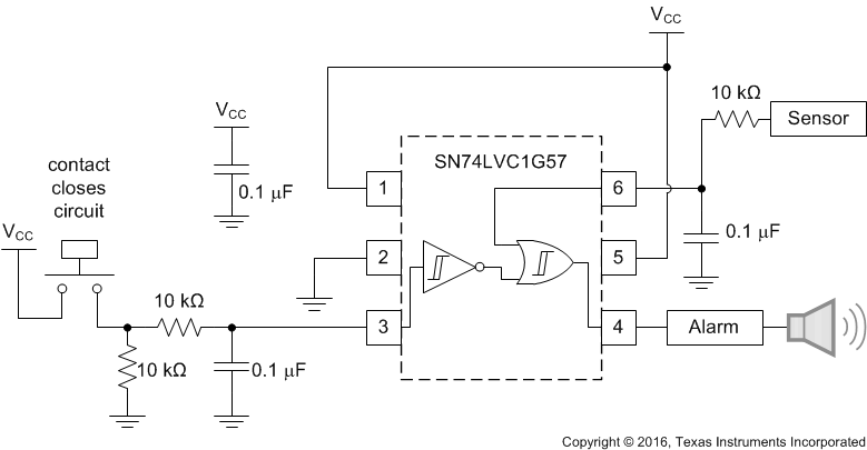
This application shows the SN74LVC1G57 configured as an OR gate with an inverted input. This particular configuration is helpful for dual sensor or switch applications where one of the inputs is normally closed or a logic high 1. Normally this application would require two external gates, but because the SN74LVC1G57 can be configured to meet this function the application can be implemented with a single chip solution.
 Figure 9. Dual-Sensor Alarm Trigger
9.2.1 Design Requirements
9.2.1.1 Application Truth Table
Because we are working with two independent alarm triggers, we need to ensure that the alarm signal is only sent whenever either condition is met. Therefore our resulting truth table will look very much like a logic OR function. However, since we are also assuming one of the conditions to always be true, i.e. a door that should remain closed, we make use of the inverted input in Table 3.
Table 3. Dual-Sensor Truth Table
| INPUTS | OUTPUT | |
|---|---|---|
| TRIGGER OR SWITCH | SENSOR | ALARM |
| L | X | H |
| H | L | L |
| X | H | H |
9.2.1.2 Schmitt-Trigger Inputs
On a normal (non-Schmitt-Trigger) input the part will switch at the same point on the rising edge and falling edge. With a slow rising edge the part will switch at the threshold. When the switch occurs it will require current from VCC. When current is forced from VCC, the VCC level can drop causing the threshold to shift. When the threshold shifts it will cross the input again causing the part to switch again. This can go on and on causing oscillation which can cause excessive current. The same thing can happen if there is noise on the input. The noise can cross the threshold multiple times and cause oscillation or multiple clocking. The solution to these problems is to use a Schmitt-Trigger type device to translate the slow or noisy edges into something faster that will meet the input rise and fall specs of the following device. A true Schmitt-Trigger input will not have rise and fall time limitations.
9.2.2 Detailed Design Procedure
- Recommended Input conditions:
- Specified high and low levels. See (VIH and VIL) in Recommended Operating Conditions.
- Inputs are overvoltage tolerant allowing them to go as high as 5.5 V at any valid VCC.
- Recommended output conditions:
- Load currents should not exceed 20 mA on the output and 50 mA total for the part.
- Outputs should not be pulled above VCC.
9.2.3 Application Curves
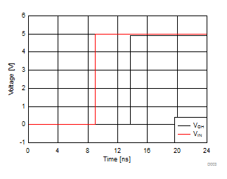
 Figure 10. Simulated Output VOH at 5 V and 25°C
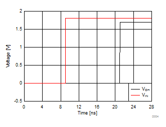
 Figure 11. Simulated Output VOH at 1.8 V and 25°C