SCES582H July 2004 – April 2015 SN74AVCH2T45
PRODUCTION DATA.
- 1 Features
- 2 Applications
- 3 Description
- 4 Revision History
- 5 Description (Continued)
- 6 Pin Configurations and Functions
-
7 Specifications
- 7.1 Absolute Maximum Ratings
- 7.2 ESD Ratings
- 7.3 Recommended Operating Conditions
- 7.4 Thermal Information
- 7.5 Electrical Characteristics
- 7.6 Switching Characteristics: VCCA = 1.2 V
- 7.7 Switching Characteristics: VCCA = 1.5 V
- 7.8 Switching Characteristics: VCCA = 1.8 V
- 7.9 Switching Characteristics: VCCA = 2.5 V
- 7.10 Switching Characteristics: VCCA = 3.3 V
- 7.11 Operating Characteristics
- 7.12 Typical Characteristics
- 8 Parameter Measurement Information
- 9 Detailed Description
- 10Application and Implementation
- 11Power Supply Recommendations
- 12Layout
- 13Device and Documentation Support
- 14Mechanical, Packaging, and Orderable Information
封装选项
请参考 PDF 数据表获取器件具体的封装图。
机械数据 (封装 | 引脚)
- DCU|8
- YZP|8
- DCT|8
散热焊盘机械数据 (封装 | 引脚)
订购信息
9 Detailed Description
9.1 Overview
This dual-bit non-inverting bus transceiver uses two separate configurable power-supply rails. The A port is designed to track VCCA and accepts any supply voltage from 1.2 V to 3.6 V. The B port is designed to track VCCB and accepts any supply voltage from 1.2 V to 3.6 V. This allows for universal low-voltage bidirectional translation and level-shifting between any of the 1.2 V, 1.5 V, 1.8 V, 2.5 V, and 3.3 V voltage nodes.
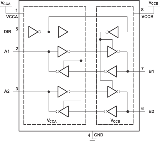
The SN74AVCH2T45 is designed for asynchronous communication between two data buses. The logic levels of the direction-control (DIR pin) input activate either the B-port outputs or the A-port outputs. The device transmits data from the A bus to the B bus when the B-port outputs are activated and from the B bus to the A bus when the A-port outputs are activated.
The SN74AVCH2T45 features active bus-hold circuitry.
The DIR input is powered by supply voltage from VCCA.
This device is fully specified for partial-power-down applications using off output current (Ioff). The Ioff circuitry disables the outputs, preventing damaging current backflow through the device when it is powered down.
The VCC isolation feature ensures that if either VCC input is at GND, both ports are put in a high-impedance state. This will prevent a false high or low logic being presented at the output.
NanoFree package technology is a major breakthrough in IC packaging concepts, using the die as the package.
9.2 Functional Block Diagram

9.3 Feature Description
9.3.1 VCC Isolation
The VCC isolation feature ensures that if either VCCA or VCCB are at GND, both ports will be in a high-impedance state (IOZ shown in the Functional Block Diagram). This prevents false logic levels from being presented to either bus.
9.3.2 2-Rail Design
Fully configurable 2-rail design allows each port to operate over the full 1.2 V to 3.6 V power-supply range.
9.3.3 IO Ports are 4.6 V Tolerant
The IO ports are up to 4.6 V tolerant
9.3.4 Partial Power Down Mode
This device is fully specified for partial-power-down applications using off output current (Ioff). The Ioff circuitry disables the outputs, preventing damaging current backflow through the device when it is powered down.
9.3.5 Bus Hold on Data Inputs
Active bus-hold circuitry holds unused or un-driven inputs at a valid logic state. TI does not recommend using pull-up or pull-down resistors with the bus-hold circuitry.
9.4 Device Functional Modes
Table 1. Function Table (Each Transceiver)
| INPUT DIR |
OPERATION |
|---|---|
| L | B data to A bus |
| H | A data to B bus |