SCES582H July 2004 – April 2015 SN74AVCH2T45
PRODUCTION DATA.
- 1 Features
- 2 Applications
- 3 Description
- 4 Revision History
- 5 Description (Continued)
- 6 Pin Configurations and Functions
-
7 Specifications
- 7.1 Absolute Maximum Ratings
- 7.2 ESD Ratings
- 7.3 Recommended Operating Conditions
- 7.4 Thermal Information
- 7.5 Electrical Characteristics
- 7.6 Switching Characteristics: VCCA = 1.2 V
- 7.7 Switching Characteristics: VCCA = 1.5 V
- 7.8 Switching Characteristics: VCCA = 1.8 V
- 7.9 Switching Characteristics: VCCA = 2.5 V
- 7.10 Switching Characteristics: VCCA = 3.3 V
- 7.11 Operating Characteristics
- 7.12 Typical Characteristics
- 8 Parameter Measurement Information
- 9 Detailed Description
- 10Application and Implementation
- 11Power Supply Recommendations
- 12Layout
- 13Device and Documentation Support
- 14Mechanical, Packaging, and Orderable Information
封装选项
请参考 PDF 数据表获取器件具体的封装图。
机械数据 (封装 | 引脚)
- DCU|8
- YZP|8
- DCT|8
散热焊盘机械数据 (封装 | 引脚)
订购信息
10 Application and Implementation
NOTE
Information in the following applications sections is not part of the TI component specification, and TI does not warrant its accuracy or completeness. TI’s customers are responsible for determining suitability of components for their purposes. Customers should validate and test their design implementation to confirm system functionality.
10.1 Application Information
The SN74AVCH2T45 is used to shift IO voltage levels from one voltage domain to another. Each bus (bus A and bus B) have independent power supplies, and a direction pin is used to control the direction of data flow.
10.2 Typical Applications
10.2.1 Unidirectional Logic Level-Shifting Application
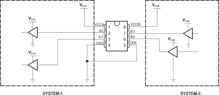
Figure 8 is an example of the SN74AVCH2T45 circuit used in a unidirectional logic level-shifting application.
 Figure 8. Unidirectional Logic Level-Shifting Application
10.2.1.1 Design Requirements
This device uses drivers which are enabled depending on the state of the DIR pin. The designer must know the intended flow of data and take care not to violate any of the high or low logic levels. Active bus-hold circuitry holds unused or un-driven inputs at a valid logic state. TI does not recommend using pull-up or pull-down resistors with the bus-hold circuitry.
10.2.1.2 Detailed Design Procedure
Table 2 lists the pins and pin descriptions of the SN74AVCH2T45 connections with SYSTEM-1 and SYSTEM-2.
Table 2. SN74AVCH2T45 Pin Connections With SYSTEM-1 and SYSTEM-2
| PIN | NAME | DESCRIPTION |
|---|---|---|
| 1 | VCCA | SYSTEM-1 supply voltage (1.2 V to 3.6 V) |
| 2 | A1 | Output level depends on VCCA. |
| 3 | A2 | Output level depends on VCCA. |
| 4 | GND | Device GND |
| 5 | DIR | The GND (low-level) determines B-port to A-port direction. |
| 6 | B2 | Input threshold value depends on VCCB. |
| 7 | B1 | Input threshold value depends on VCCB. |
| 8 | VCCB | SYSTEM-2 supply voltage (1.2 V to 3.6 V) |
10.2.1.3 Application Curve
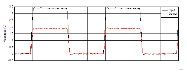
 Figure 9. 3.3- to 1.8-V Level-Shifting With 1-MHz Square Wave
10.2.2 Bidirectional Logic Level-Shifting Application
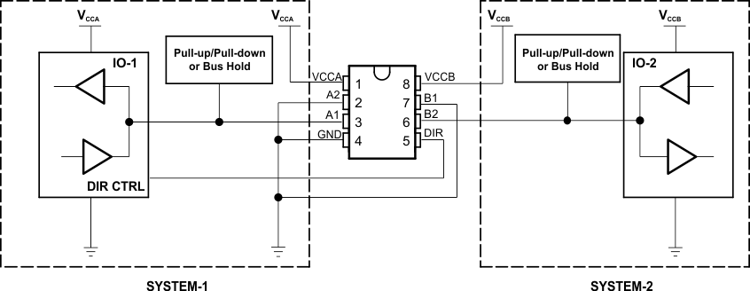
Figure 10 shows the SN74AVCH2T45 used in a bidirectional logic level-shifting application. Because the SN74AVCH2T45 does not have an output-enable (OE) pin, system designers should take precautions to avoid bus contention between SYSTEM-1 and SYSTEM-2 when changing directions.
 Figure 10. Bidirectional Logic Level-Shifting Application
10.2.2.1 Design Requirements
This device uses drivers which are enabled depending on the state of the DIR pin. The designer must know the intended flow of data and take care not to violate any of the high or low logic levels. Active bus-hold circuitry holds unused or un-driven inputs at a valid logic state. TI does not recommend using pull-up or pull-down resistors with the bus-hold circuitry.
10.2.2.2 Detailed Design Procedure
Table 3 lists a sequence that shows data transmission from SYSTEM-1 to SYSTEM-2 and then from SYSTEM-2 to SYSTEM-1.
Table 3. Data Transmission Sequence
| STATE | DIR CTRL | IO-1 | IO-2 | DESCRIPTION |
|---|---|---|---|---|
| 1 | H | Output | Input | SYSTEM-1 data to SYSTEM-2 |
| 2 | H | Hi-Z | Hi-Z | SYSTEM-2 is getting ready to send data to SYSTEM-1. IO-1 and IO-2 are disabled. The bus-line state depends on pull-up or pull-down.(1) |
| 3 | L | Hi-Z | Hi-Z | DIR bit is flipped. IO-1 and IO-2 still are disabled. The bus-line state depends on pull-up or pull-down.(1) |
| 4 | L | Input | Output | SYSTEM-2 data to SYSTEM-1 |
10.2.2.2.1 Enable Times
Calculate the enable times for the SN74AVCH2T45 using the following formulas:
In a bidirectional application, these enable times provide the maximum delay from the time the DIR bit is switched until an output is expected. For example, if the SN74AVCH2T45 initially is transmitting from A to B, the DIR bit is switched; the B port of the device must be disabled before presenting it with an input. After the B port has been disabled, an input signal applied to it appears on the corresponding A port after the specified propagation delay.
10.2.2.3 Application Curve
Refer to Figure 9.