SCES595N JULY   2004  – July 2017 SN74AUP1G125

UNLESS OTHERWISE NOTED, this document contains PRODUCTION DATA.  

  1. Features
  2. Applications
  3. Description
  4. Revision History
  5. Pin Configuration and Functions
  6. Specifications
    1. 6.1  Absolute Maximum Ratings
    2. 6.2  ESD Ratings
    3. 6.3  Recommended Operating Conditions
    4. 6.4  Thermal Information
    5. 6.5  Electrical Characteristics, TA = 25°C
    6. 6.6  Electrical Characteristics, TA = -40°C to +85°C
    7. 6.7  Switching Characteristics, CL = 5 pF
    8. 6.8  Switching Characteristics, CL = 10 pF
    9. 6.9  Switching Characteristics, CL = 15 pF
    10. 6.10 Switching Characteristics, CL = 30 pF
    11. 6.11 Operating Characteristics
    12. 6.12 Typical Characteristics
  7. Parameter Measurement Information
  8. Detailed Description
    1. 8.1 Overview
    2. 8.2 Functional Block Diagram
    3. 8.3 Feature Description
      1. 8.3.1 Balanced High-Drive CMOS Push-Pull Outputs
      2. 8.3.2 Standard CMOS Inputs
      3. 8.3.3 Clamp Diodes
      4. 8.3.4 Partial Power Down (Ioff)
      5. 8.3.5 Over-voltage Tolerant Inputs
    4. 8.4 Device Functional Modes
  9. Application and Implementation
    1. 9.1 Application Information
    2. 9.2 Typical Application
      1. 9.2.1 Design Requirements
      2. 9.2.2 Detailed Design Procedure
      3. 9.2.3 Application Curve
  10. 10Power Supply Recommendations
  11. 11Layout
    1. 11.1 Layout Guidelines
    2. 11.2 Layout Example
  12. 12Device and Documentation Support
    1. 12.1 Documentation Support
      1. 12.1.1 Related Documentation
    2. 12.2 Receiving Notification of Documentation Updates
    3. 12.3 Community Resources
    4. 12.4 Trademarks
    5. 12.5 Electrostatic Discharge Caution
    6. 12.6 Glossary
  13. 13Mechanical, Packaging, and Orderable Information

封装选项

机械数据 (封装 | 引脚)
散热焊盘机械数据 (封装 | 引脚)
订购信息

Pin Configuration and Functions

DBV Package
5-Pin SOT-23
Top View
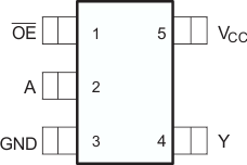
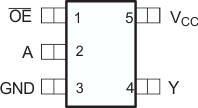
SN74AUP1G125 pinout_dbv_SCES595.gif
DRL Package
5-Pin SOT
Top View
SN74AUP1G125 pinout_drl_SCES595.gif
YZP or YZT Package
5-Pin DSBGA
Bottom View
SN74AUP1G125 SN74AUP1G125-YZP-pinout.gif
DCK Package
5-Pin SC70
Top View
SN74AUP1G125 pinout_dck_SCES595.gif
DSF Package
6-Pin SON
Top View
SN74AUP1G125 pinout_dsf_SCES595.gif
DRY Package
6-Pin SON
Top View
SN74AUP1G125 pinout_dry_SCES595.gif
YFP Package
6-Pin DSBGA
Bottom View
SN74AUP1G125 SN74AUP1G125-YFP-pinout.gif
DPW Package
5-Pin X2SON
Top View
SN74AUP1G125 DPW_Pinout.gif

Pin Functions

PIN I/O DESCRIPTION
NAME SOT-23 (DBV), SC70 (DCK), SOT (DRL), X2SON (DPW) SON (DRY or DSF) DSBGA (YZP or YZT) DSBGA (YFP)
A 2 2 B1 B1 I Input
DNU B2 Do not use
GND 3 3 C1 C1 Ground
N.C. 5 No connection
OE 1 1 A1 A1 I Output enable (active low)
VCC 5 6 A2 A2 Positive supply
Y 4 4 C2 C2 O Output