ZHCSVZ9H June 1998 – April 2024 SN74AHC594
PRODMIX
- 1
- 1 特性
- 2 应用
- 3 说明
- 4 Pin Configuration and Functions
-
5 Specifications
- 5.1 Absolute Maximum Ratings
- 5.2 ESD Ratings
- 5.3 Recommended Operating Conditions
- 5.4 Thermal Information
- 5.5 Electrical Characteristics
- 5.6 Timing Requirements, VCC = 3.3 V ± 0.3 V
- 5.7 Timing Requirements, VCC = 5 V ± 0.5 V
- 5.8 Switching Characteristics, VCC = 3.3 V ± 0.3 V
- 5.9 Switching Characteristics, VCC = 5 V ± 0.5 V
- 5.10 Noise Characteristics
- 5.11 Operating Characteristics
- 5.12 Typical Characteristics
- 6 Parameter Measurement Information
- 7 Detailed Description
- 8 Application and Implementation
- 9 Device and Documentation Support
- 10Revision History
- 11Mechanical, Packaging, and Orderable Information
封装选项
请参考 PDF 数据表获取器件具体的封装图。
机械数据 (封装 | 引脚)
- PW|16
- DB|16
- NS|16
- N|16
- D|16
散热焊盘机械数据 (封装 | 引脚)
订购信息
5.7 Timing Requirements, VCC = 5 V ± 0.5 V
over recommended operating free-air temperature range (unless
otherwise noted) (see Load Circuit and Voltage Waveforms)
| TA = 25°C | SN54AHC594(2) | SN74AHC594 | UNIT | ||||||
|---|---|---|---|---|---|---|---|---|---|
| MIN | MAX | MIN | MAX | MIN | MAX | ||||
| tw | Pulse Duration | RCLK or SRCLK high or low | 5 | 5 | 5 | ns | |||
| RCLR or SRCLR low | 5.2 | 5.2 | 5.2 | ||||||
| tsu | Setup time | SER before SRCLK↑ | 3 | 3 | 3 | ns | |||
| SRCLK↑ before RCLK↑(1) | 5 | 5 | 5 | ||||||
| SRCLR low before SRCLK↑ | 5 | 5 | 5 | ||||||
| SRCLR high (inactive) before SRCLK↑ | 2.9 | 3.3 | 3.3 | ||||||
| RCLR high (inactive) before RCLK↑ | 3.2 | 3.7 | 3.7 | ||||||
| th | Hold time, data after CLK↑ | SER after SRCLK↑ | 2 | 2 | 2 | ns | |||
(1) This setup time allows the storage register to receive stable data from the shift register. The clocks can be tied together, in which case the shift register is one clock pulse ahead of the storage register.
(2) Product Preview
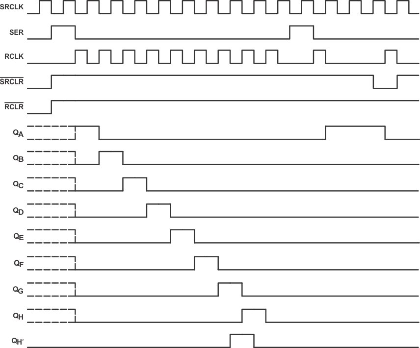
 Figure 5-1 Timing Diagram