SLLS881G December 2007 – October 2014 SN65LVDS315
PRODUCTION DATA.
- 1 Features
- 2 Applications
- 3 Description
- 4 Revision History
- 5 Pin Configuration and Functions
- 6 Specifications
- 7 Parameter Measurement Information
-
8 Detailed Description
- 8.1 Overview
- 8.2 Functional Block Diagram
- 8.3
Feature Description
- 8.3.1 Frame Counter Size
- 8.3.2 Data Formats
- 8.3.3 Parallel Input Port Timing Information
- 8.3.4 MIPI CSI-1 / CCP2-Class 0 Interface
- 8.3.5 Frame Structure and Synchronization Codes
- 8.3.6 Preventing Wrong Synchronization
- 8.3.7 Frame Structure
- 8.3.8 VS and HS Timing to Generate the Correct Control Signals
- 8.4 Device Functional Modes
- 9 Application and Implementation
- 10Power Supply Recommendations
- 11Layout
- 12Device and Documentation Support
- 13Mechanical, Packaging, and Orderable Information
1 Features
- MIPI CSI-1 and SMIA CCP Support
- Connects Directly to OMAP CSI Interface
- 4×4 mm QFN Package
- ESD Rating >3 kV (HBM) Camera Input Ports
and >2 kV (HBM) All Other Ports - Pixel Clock Range 3.5–27 MHz
- Three Operating Modes to Conserve Power
- Active Mode VGA Camera 30 fps: 7 mA
- Typical Shutdown and Standby: 0.5 μA
- Operating Temperature Range –40°C to 85°C
- Input Data Voltage Range From 1.8 V to 3.3 V
- EMI
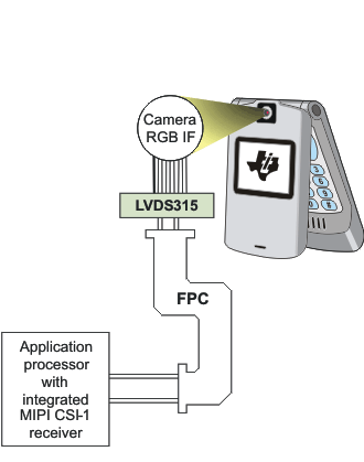
2 Applications
- Camera to Host Controller (e.g. OMAP2420, OMAP2430, OMAP3430)
- Mobile Phones and Smart Phones
3 Description
The SN65LVDS315 is a camera serializer that converts 8-bit parallel camera data into MIPI-CSI1 or SMIA CCP compliant serial signals.
The device converts the parallel 8-bit data to two sub-low-voltage differential signaling (SubLVDS) serial data and clock output. Meanwhile the serialized data is presented on the differential serial data output DOUT with a differential clock signal on output CLK. Where The frequency of CLK is 8x DCLK input pixel clock rate.
The SN65LVDS315 supports three power modes (Shutdown, standby and active) to conserve power.
All CMOS inputs offer failsafe operation to protect the input from damage during power up and to avoid current flow into the device inputs during power up. The core supply of the SN65LVDS315 is 1.8 V. To provide greater flexibility, the camera data inputs support a supply range from 1.8 V to 3.3 V and the device is characterized for operation over ambient air temperatures of –40°C to 85°C.
Device Information(1)
| PART NUMBER | PACKAGE | BODY SIZE (NOM) |
|---|---|---|
| SN65LVDS315 | VQFN (24) | 4.00 mm x 4.00 mm |
- For all available packages, see the orderable addendum at the end of the datasheet.