SLLS804D March 2009 – August 2016 SN65HVDA540-5-Q1 , SN65HVDA540-Q1 , SN65HVDA541-5-Q1 , SN65HVDA541-Q1 , SN65HVDA542-5-Q1 , SN65HVDA542-Q1
PRODUCTION DATA.
- 1 Features
- 2 Applications
- 3 Description
- 4 Revision History
- 5 Pin Configuration and Functions
- 6 Specifications
- 7 Parameter Measurement Information
- 8 Detailed Description
- 9 Application and Implementation
- 10Power Supply Recommendations
- 11Layout
- 12Device and Documentation Support
- 13Mechanical, Packaging, and Orderable Information
9 Application and Implementation
NOTE
Information in the following applications sections is not part of the TI component specification, and TI does not warrant its accuracy or completeness. TI’s customers are responsible for determining suitability of components for their purposes. Customers should validate and test their design implementation to confirm system functionality.
9.1 Application Information
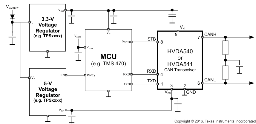
These CAN transceivers are typically used in applications with a host microprocessor or FPGA that includes the data link layer portion of the CAN protocol. Below are typical application configurations for both 5-V and 3.3-V microprocessor applications. The bus termination is shown for illustrative purposes.
9.2 Typical Applications
9.2.1 3.3-V I/O Voltage Level and Normal Mode
9.2.1.1 Design Requirements
The ISO 11898-2 Standard specifies a maximum bus length of 40 m and maximum stub length of 0.3 m. However, with careful design, users can have longer cables, longer stub lengths, and many more nodes to a bus. A large number of nodes requires transceivers with high input impedance such as the HVDA54x family of transceivers.
Many CAN organizations and standards have scaled the use of CAN for applications outside the original ISO 11898-2. They have made system-level tradeoffs for data rate, cable length, and parasitic loading of the bus. Examples of some of these specifications are ARINC825, CANopen, DeviceNet, and NMEA2000.
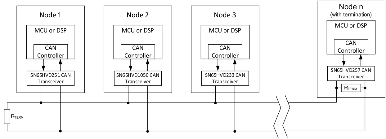 Figure 20. Typical CAN Bus
9.2.1.2 Detailed Design Procedure
The ISO 11898 standard specifies the interconnect to be a twisted pair cable (shielded or unshielded) with
120-Ω characteristic impedance (ZO). Resistors equal to the characteristic impedance of the line should be used to terminate both ends of the cable to prevent signal reflections. Unterminated drop lines (stubs) connecting nodes to the bus should be kept as short as possible to minimize signal reflections. The termination may be on the cable or in a node, but if nodes may be removed from the bus, the termination must be carefully placed so that two terminations always exist on the network. Termination may be a single 120-Ω resistor at the end of the bus, either on the cable or in a terminating node. If filtering and stabilization of the common mode voltage of the bus is desired, then split termination may be used (see Figure 21). Split termination improves the electromagnetic emissions behavior of the network by eliminating fluctuations in the bus common-mode voltages at the start and end of message transmissions.
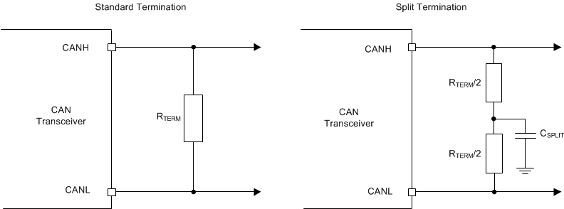 Figure 21. CAN Bus Termination Concepts
The family of transceivers have variants for both 5-V only applications and applications where level shifting is needed for a 3.3-V micrcontroller.
9.2.1.2.1 Loop Propagation Delay
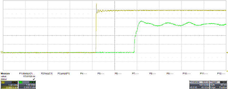
Transceiver loop delay is a measure of the overall device propagation delay and consists of the delay from driver input (TXD pin) to differential outputs (CANH and CANL), plus the delay from the receiver inputs (CANH and CANL) to the output pin RXD.
In Figure 22 is displayed the loop delay at 1 Mbps with Vio equal to 3.3 V
9.2.1.3 Application Curves
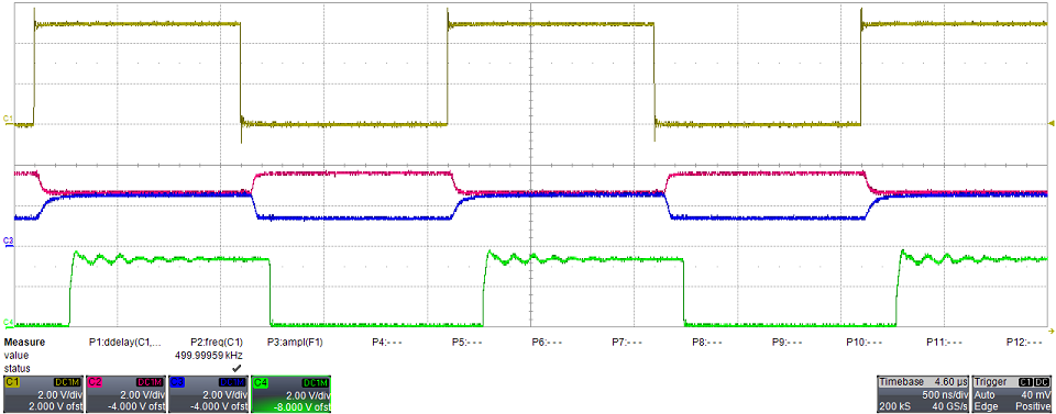
STB = 0, VIO = 3.3 V.
1 Mbps
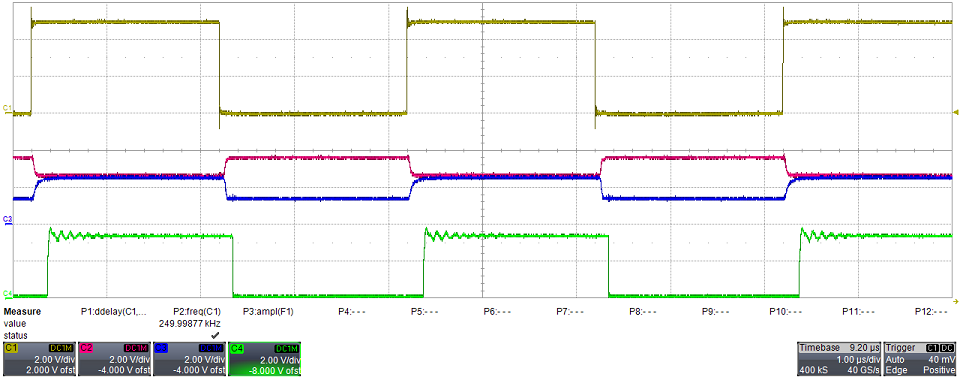
STB = 0, VIO = 3.3 V.
500 Kbps
9.3 System Examples
Figure 25, Figure 26, and Figure 27 show three different example applications using the HVDA54x family of transceivers. Different devices and configurations can be used depending on the I/O voltage levels supported by the MCU and different operating modes required by the end application.
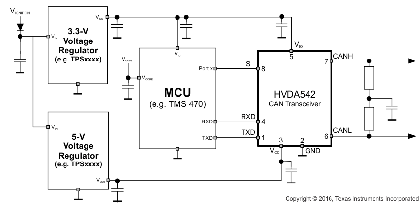 Figure 25. Typical Application Using 3.3-V I/O Voltage Level and No Low-Power Mode
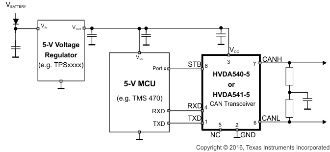 Figure 26. Typical Application Using 5-V MCU and Low-Power Mode
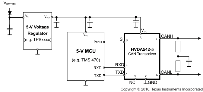 Figure 27. Typical Application Using 5-V MCU and No Low-Power Mode