SLLS995D February   2010  – May 2015 SN65HVDA1040A-Q1

PRODUCTION DATA.  

  1. Features
  2. Applications
  3. Description
  4. Revision History
  5. Pin Configuration and Functions
  6. Specifications
    1. 6.1 Absolute Maximum Ratings
    2. 6.2 ESD Ratings
    3. 6.3 Recommended Operating Conditions
    4. 6.4 Thermal Information
    5. 6.5 Electrical Characteristics
    6. 6.6 Power Dissipation Characteristics
    7. 6.7 Switching Characteristics
    8. 6.8 Typical Characteristics
  7. Parameter Measurement Information
  8. Detailed Description
    1. 8.1 Overview
    2. 8.2 Functional Block Diagram
    3. 8.3 Feature Description
      1. 8.3.1 Operating Modes
        1. 8.3.1.1 Bus States by Mode
        2. 8.3.1.2 Normal Mode
        3. 8.3.1.3 Standby Mode and RXD Wake-Up Request
      2. 8.3.2 Protection Features
        1. 8.3.2.1 TXD Dominant State Time-Out
        2. 8.3.2.2 Thermal Shutdown
        3. 8.3.2.3 Undervoltage Lockout and Unpowered Device
    4. 8.4 Device Functional Modes
  9. Application and Implementation
    1. 9.1 Application Information
      1. 9.1.1 Using With 3.3-V Microcontrollers
      2. 9.1.2 Using SPLIT With Split Termination
    2. 9.2 Typical Application
      1. 9.2.1 Design Requirements
        1. 9.2.1.1 Bus Loading, Length, and Number of Nodes
        2. 9.2.1.2 CAN Termination
        3. 9.2.1.3 Loop Propagation Delay
      2. 9.2.2 Detailed Design Procedure
        1. 9.2.2.1 Transient Voltage Suppresser (TVS) Diodes
      3. 9.2.3 Application Curves
  10. 10Power Supply Recommendations
  11. 11Layout
    1. 11.1 Layout Guidelines
    2. 11.2 Layout Example
    3. 11.3 PCB and Thermal Considerations for VSON Package
    4. 11.4 ESD Protection
  12. 12Device and Documentation Support
    1. 12.1 Documentation Support
      1. 12.1.1 Related Documentation
    2. 12.2 Community Resources
    3. 12.3 Trademarks
    4. 12.4 Electrostatic Discharge Caution
    5. 12.5 Glossary
  13. 13Mechanical, Packaging, and Orderable Information

封装选项

机械数据 (封装 | 引脚)
散热焊盘机械数据 (封装 | 引脚)
订购信息

5 Pin Configuration and Functions

D Package
8-Pin SOIC
Top View
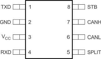
SN65HVDA1040A-Q1 pinout_01_lls995.gif
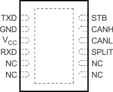
DSG Package
12-Pin VSON
Top View
SN65HVDA1040A-Q1 pinout_02_lls995.gif

Pin Functions

PIN TYPE DESCRIPTION
NAME SOIC VSON
TXD 1 1 I CAN transmit data input (low for dominant bus state, high for recessive bus state)
GND 2 2 GND Ground connection
VCC 3 3 Supply Transceiver 5-V supply voltage input
RXD 4 4 O CAN receive data output (low in domonint bus state, high in recessive bus state)
SPLIT 5 9 O Common-mode stabilization output
CANL 6 10 I/O Low-level CAN bus line
CANH 7 11 I/O High-level CAN bus line
STB 8 12 I Standby mode select pin (active high)
NC 5-8 NC No connect