SLLS995D February 2010 – May 2015 SN65HVDA1040A-Q1
PRODUCTION DATA.
- 1 Features
- 2 Applications
- 3 Description
- 4 Revision History
- 5 Pin Configuration and Functions
- 6 Specifications
- 7 Parameter Measurement Information
- 8 Detailed Description
- 9 Application and Implementation
- 10Power Supply Recommendations
- 11Layout
- 12Device and Documentation Support
- 13Mechanical, Packaging, and Orderable Information
封装选项
机械数据 (封装 | 引脚)
散热焊盘机械数据 (封装 | 引脚)
- DSJ|12
订购信息
7 Parameter Measurement Information
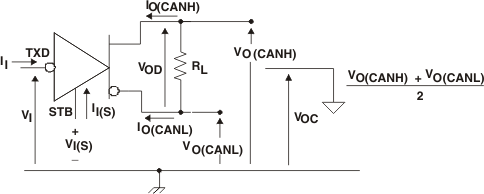 Figure 3. Driver Voltage, Current, and Test Definition
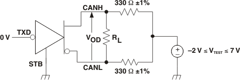 Figure 4. Driver VOD Test Circuit
 Figure 5. Driver Test Circuit and Voltage Waveforms
 Figure 6. Receiver Voltage and Current Definitions

A. The input pulse is supplied by a generator having the following characteristics: PRR ≤ 125 kHz, 50% duty cycle, tr ≤ 6 ns, tf ≤ 6 ns, ZO = 50 Ω.
B. CL includes instrumentation and fixture capacitance within ±20%.
Figure 7. Receiver Test Circuit and Voltage Waveforms
Table 1. Differential Input Voltage Threshold Test
| INPUT | OUTPUT R |
|||
|---|---|---|---|---|
| VCANH | VCANL | |VID| | ||
| –11.1 V | –12 V | 900 mV | L | VOL |
| 12 V | 11.1 V | 900 mV | L | |
| –6 V | –12 V | 6 V | L | |
| 12 V | 6 V | 6 V | L | |
| –11.5 V | –12 V | 500 mV | H | VOH |
| 12 V | 11.5 V | 500 mV | H | |
| –12 V | –6 V | 6 V | H | |
| 6 V | 12 V | 6 V | H | |
| Open | Open | X | H | |

A. CL = 100 pF and includes instrumentation and fixture capacitance within ±20%.
B. All VI input pulses are supplied by a generator having the following characteristics: tr or tf ≤ 6 ns, pulse repetition rate (PRR) = 125 kHz, 50% duty cycle.
Figure 8. ten Test Circuit and Waveforms

NOTE:
All VI input pulses are from 0 V to VCC and supplied by a generator having the following characteristics: tr or tf ≤ 6 ns, pulse repetition rate (PRR) = 125 kHz, 50% duty cycle.
A. CL = 100 pF and includes instrumentation and fixture capacitance within ±20%.
B. All VI input pulses are from 0 V to VCC and supplied by a generator having the following characteristics: tr or tf ≤ 6 ns, pulse repetition rate (PRR) = 125 kHz, 50% duty cycle.
Figure 10. t(LOOP) Test Circuit and Waveforms

A. All VI input pulses are from 0 V to VCC and supplied by a generator having the following characteristics: tr or tf ≤ 6 ns, pulse repetition rate (PRR) = 500 Hz, 50% duty cycle.
B. CL = 100 pF includes instrumentation and fixture capacitance within ±20%.
Figure 11. Dominant Time-Out Test Circuit and Waveforms
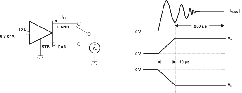 Figure 12. Driver Short-Circuit Current Test and Waveforms

A. For VI bit width ≤ 0.7 µs, VO = VOH. For VI bit width ≥ 5 µs, VO = VOL. VI input pulses are supplied from a generator with the following characteristics: tr/tf < 6 ns.
B. CL = 15 pF and includes instrumentation and fixture capacitance within ±20%.
Figure 13. tBUS Test Circuit and Waveforms
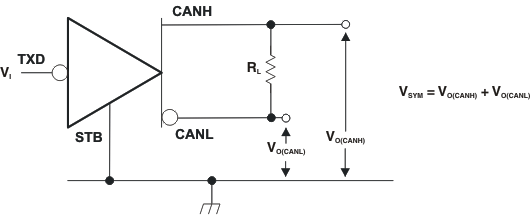
A. All VI input pulses are from 0 V to VCC and supplied by a generator having the following characteristics: tr/tf ≤ 6 ns, pulse repetition rate (PRR) = 250 kHz, 50% duty cycle.
Figure 14. Driver Output Symmetry Test Circuit
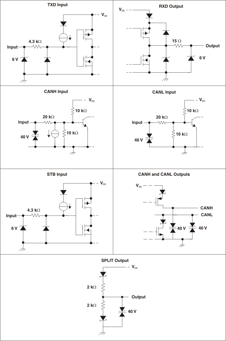 Figure 15. Equivalent Input and Output Schematic Diagrams