ZHCS378C September 2011 – March 2015 SN65HVD62
PRODUCTION DATA.
9 Detailed Description
9.1 Overview
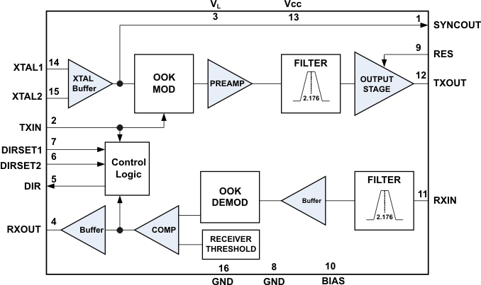
If DIRSET1 and DIRSET2 are in a logic High state, the device will be in STANDBY mode. While in STANDBY mode, the Receiver functions normally, detecting carrier frequency activity on the RXIN pin and setting the RXOUT state as discussed below. But the Transmitter circuits are not active in STANDBY, thus the TXOUT pin is idle regardless of the logic state of TXIN. The supply current in STANDBY mode is significantly reduced, allowing power savings when the node is not transmitting.
9.2 Functional Block Diagram

9.3 Device Functional Modes
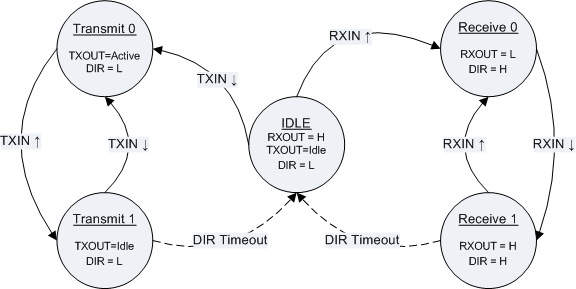
When not in STANDBY mode, the default power-on state is IDLE. When in IDLE mode, RXOUT is High, and TXOUT is quiet. The device transitions to RECEIVE mode when a valid modulated signal is detected on the RXIN line <OR> the device transitions to TRANSMIT mode when TXIN goes Low. The device stays in either RECEIVE or TRANSMIT mode until DIR Timeout (nominal 16 bit times) after the last activity on RXOUT or TXIN.
When in RECEIVE mode:
- RXOUT responds to all valid modulated signals on RXIN, whether from the local transmitter, a remote transmitter, or long noise burst.
- TXOUT responds to TXIN, generating 2.176 MHz signals on TXOUT when TXIN is Low, and TXOUT is quiet when TXIN is High. (In normal operation, TXIN is expected to remain High when the device is in RECEIVE mode).
- The device stays in RECEIVE mode until 16 bit times after the last rising edge on RXOUT, caused by valid modulated signal on the RXIN line.
When in TRANSMIT mode:
- RXOUT stays High, regardless of the input signal on RXIN.
- TXOUT responds to TXIN, generating 2.176 MHz signals on TXOUT when TXIN is Low, and TXOUT is quiet when TXIN is High.
- The device stays in TRANSMIT mode until 16 bit times after TXIN goes High.
Table 1. Driver Function Table(1)
| TXIN | [DIRSET1, DIRSET2] | TXOUT | COMMENT |
|---|---|---|---|
| H | [L,L], [L,H] or [H,L] | < 1 mVPP at 2.176 MHz | Driver not active |
| L | VOPP at 2.176 MHz | Driver active | |
| X | [H,H] | < 1 mVPP at 2.176 MHz | Standby mode |
Table 2. Receiver and DIR Function Table(1)
| RXIN | RXOUT | DIR | COMMENT (see Figure 22) |
|---|---|---|---|
| IDLE mode (not transmitting or receiving) | |||
| < VIT at 2.176 MHz for longer than DIR timeout | H | L | No outgoing or incoming signal |
| RECEIVE mode (not already transmitting) | |||
| < VIT at 2.176 MHz for less than tDIR Timeout | H | H | Incoming '1' bit, DIR stays HIGH for DIR Timeout |
| > VIT at 2.176 MHz for longer than tnoise filter | L | H | Incoming '0' bit, DIR output is HIGH |
| TRANSMIT mode (not already receiving) | |||
| X | H | L | Outgoing message, DIR stays LOW for DIR Timeout |
 Figure 22. State Transition Diagram