ZHCSES3C March   2016  – August 2019 SN65DPHY440SS , SN75DPHY440SS

PRODUCTION DATA.  

  1. 特性
  2. 应用
  3. 说明
    1.     Device Images
      1.      简化原理图
      2.      典型应用
  4. 修订历史记录
  5. Pin Configuration and Functions
    1.     Pin Functions
  6. Specifications
    1. 6.1 Absolute Maximum Ratings
    2. 6.2 ESD Ratings
    3. 6.3 Recommended Operating Conditions
    4. 6.4 Thermal Information
    5. 6.5 Electrical Characteristics, Power Supply
    6. 6.6 Electrical Characteristics
    7. 6.7 Timing Requirements
    8. 6.8 Switching Characteristics
    9. 6.9 Typical Characteristics
  7. Detailed Description
    1. 7.1 Overview
    2. 7.2 Functional Block Diagram
    3. 7.3 Feature Description
      1. 7.3.1 HS Receive Equalization
      2. 7.3.2 HS TX Edge Rate Control
      3. 7.3.3 TX Voltage Swing and Pre-Emphasis Control
      4. 7.3.4 Dynamic De-skew
    4. 7.4 Device Functional Modes
      1. 7.4.1 Shutdown Mode
      2. 7.4.2 LP Mode
      3. 7.4.3 ULPS Mode
      4. 7.4.4 HS Mode
    5. 7.5 Register Maps
      1. 7.5.1  BIT Access Tag Conventions
      2. 7.5.2  Standard CSR Registers (address = 0x000 - 0x07)
        1. Table 6. Standard CSR Registers (0x000 - 0x07)
      3. 7.5.3  Standard CSR Register (address = 0x08)
        1. Table 7. Standard CSR Register (0x08)
      4. 7.5.4  Standard CSR Register (address = 0x09)
        1. Table 8. Standard CSR Register (0x09)
      5. 7.5.5  Standard CSR Register (address = 0x0A)
        1. Table 9. Standard CSR Register (0x0A)
      6. 7.5.6  Standard CSR Register (address = 0x0B)
        1. Table 10. Standard CSR Register (0x0B)
      7. 7.5.7  Standard CSR Register (address = 0x0D)
        1. Table 11. Standard CSR Register (0x0D)
      8. 7.5.8  Standard CSR Register (address = 0x0E)
        1. Table 12. Standard CSR Register (0x0E)
      9. 7.5.9  Standard CSR Register (address = 0x10) [reset = 0xFF]
        1. Table 13. Standard CSR Register (0x10)
      10. 7.5.10 Standard CSR Register (address = 0x11) [reset = 0xFF]
        1. Table 14. Standard CSR Register (0x11)
  8. Application and Implementation
    1. 8.1 Application Information,
    2. 8.2 Typical Application, CSI-2 Implementations
      1. 8.2.1 Design Requirements
      2. 8.2.2 Detailed Design Procedure
        1. 8.2.2.1 Reset Implementation
      3. 8.2.3 Application Curves
  9. Power Supply Recommendations
  10. 10Layout
    1. 10.1 Layout Guidelines
    2. 10.2 Layout Example
  11. 11器件和文档支持
    1. 11.1 相关链接
    2. 11.2 社区资源
    3. 11.3 商标
    4. 11.4 静电放电警告
    5. 11.5 Glossary
  12. 12机械、封装和可订购信息

封装选项

机械数据 (封装 | 引脚)
散热焊盘机械数据 (封装 | 引脚)
订购信息

Typical Application, CSI-2 Implementations

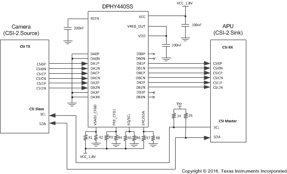
The DPHY440 supports 4 CSI-2 DPHY lanes plus a clock. Unlike DSI, CSI-2 does not have a back channel path. Because of this, there is no requirement on lane ordering. Because there is no lane ordering requirement, there are more combinations which can be implemented. All possible combinations are supported by the DPHY440. For all CSI-2 implementations, the polarity must be maintained between the CSI-2 Source and CSI-2 Sink. The DPHY440 does not support polarity inversion.

SN65DPHY440SS SN75DPHY440SS CSI2_Imple_application_sllseo9.gifFigure 17. CSI-2 Example: Typical SNx5DPHY440SS Placement in the System
SN65DPHY440SS SN75DPHY440SS CSI2_two_lane_example_sllseo9.gifFigure 18. CSI-2 Two Lane Example