ZHCSUM2G March 1993 – February 2024 SN65C1167 , SN65C1168 , SN75C1167 , SN75C1168
PRODUCTION DATA
4 Pin Configuration and Functions
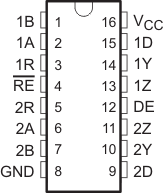
 Figure 4-1 SN65C1167: DB or NS Package
SN75C1167: DB, N, or NS Package
(Top View)
Table 4-1 Pin Functions, SNx5C1167
| PIN | TYPE(1) | DESCRIPTION | |
|---|---|---|---|
| NAME | NO. | ||
| 1B | 1 | I | Inverting Input of Channel 1 Differential Receiver |
| 1A | 2 | I | Non-Inverting Input of Channel 1 Differential Receiver |
| 1R | 3 | O | Single Ended Receiver Output for Channel 1 |
| RE | 4 | I | Receiver Active Low Enable Input for Channel 1 and 2 |
| 2R | 5 | O | Single Ended Receiver Output for Channel 2 |
| 2A | 6 | I | Non-Inverting Input of Channel 1 Differential Receiver |
| 2B | 7 | I | Inverting Input of Channel 2 Differential Receiver |
| GND | 8 | G | Device Ground |
| 2D | 9 | I | Single Ended Driver Input for Channel 2 |
| 2Y | 10 | O | Non-Inverting Output of Channel 2 Differential Driver |
| 2Z | 11 | O | Inverting Output of Channel 2 Differential Driver |
| DE | 12 | I | Driver Active High Enable Input for Channel 1 and 2 |
| 1Z | 13 | O | Inverting Output of Channel 1 Differential Driver |
| 1Y | 14 | O | Non-Inverting Output of Channel 1 Differential Driver |
| 1D | 15 | I | Single Ended Driver Input for Channel 1 |
| VCC | 16 | P | Device VCC, connect 4.5V to 5.5V Source between this Pin and Device Ground |
(1) I = Input, O = Output, I/O = Input or Output, G = Ground, P = Power.
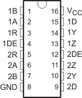
 Figure 4-2 SN65C1168: N, NS, or PW Package
SN75C1168: DB, N, NS, or PW Package
(Top View)
Table 4-2 Pin Functions, SNx5C1168
| PIN | TYPE(1) | DESCRIPTION | |
|---|---|---|---|
| NAME | NO. | ||
| 1B | 1 | I | Inverting Input of Channel 1 Differential Receiver |
| 1A | 2 | I | Non-Inverting Input of Channel 1 Differential Receiver |
| 1R | 3 | O | Single Ended Receiver Output for Channel 1 |
| 1DE | 4 | I | Driver Active High Enable Input for Channel 1 |
| 2R | 5 | O | Single Ended Receiver Output for Channel 2 |
| 2A | 6 | I | Non-Inverting Input of Channel 1 Differential Receiver |
| 2B | 7 | I | Inverting Input of Channel 2 Differential Receiver |
| GND | 8 | G | Device Ground |
| 2D | 9 | I | Single Ended Driver Input for Channel 2 |
| 2Y | 10 | O | Non-Inverting Output of Channel 2 Differential Driver |
| 2Z | 11 | O | Inverting Output of Channel 2 Differential Driver |
| 2DE | 12 | I | Driver Active High Enable Input for Channel 2 |
| 1Z | 13 | O | Inverting Output of Channel 1 Differential Driver |
| 1Y | 14 | O | Non-Inverting Output of Channel 1 Differential Driver |
| 1D | 15 | I | Single Ended Driver Input for Channel 1 |
| VCC | 16 | P | Device VCC, connect 4.5V to 5.5V Source between this Pin and Device Ground |
(1) I = Input, O = Output, I/O = Input or Output, G = Ground, P = Power.