ZHCSND7 September   2022 SN6507-Q1

PRODUCTION DATA  

  1. 特性
  2. 应用
  3. 说明
  4. Revision History
  5. Pin Configuration and Functions
  6. Specifications
    1. 6.1 Absolute Maximum Ratings
    2. 6.2 ESD Ratings
    3. 6.3 Recommended Operating Conditions
    4. 6.4 Thermal Information
    5. 6.5 Electrical Characteristics
    6. 6.6 Switching Characteristics
    7. 6.7 Typical Characteristics, SN6507-Q1
  7. Parameter Measurement Information
  8. Detailed Description
    1. 8.1 Overview
    2. 8.2 Functional Block Diagram
    3. 8.3 Feature Description
      1. 8.3.1 Push-Pull Converter
      2. 8.3.2 Core Magnetization
      3. 8.3.3 Duty Cycle Control
      4.      Programmable Switching Frequency
      5. 8.3.4 Spread Spectrum Clocking
      6. 8.3.5 Slew Rate Control
      7. 8.3.6 Protection Features
        1. 8.3.6.1 Over Voltage Protection (OVP)
        2. 8.3.6.2 Over Current and Short Circuit Protection (OCP)
        3. 8.3.6.3 Under Voltage Lock-Out (UVLO)
        4. 8.3.6.4 Thermal Shut Down (TSD)
    4. 8.4 Device Functional Modes
      1. 8.4.1 Start-Up Mode
        1. 8.4.1.1 Soft-Start
      2. 8.4.2 Operation Mode
      3. 8.4.3 Shutdown Mode
      4. 8.4.4 SYNC Mode
  9. Application and Implementation
    1. 9.1 Application Information
    2. 9.2 Typical Application
      1. 9.2.1 Design Requirements
      2. 9.2.2 Detailed Design Procedure
        1. 9.2.2.1 Pin Configuration
        2. 9.2.2.2 LDO Selection
        3. 9.2.2.3 Diode Selection
        4. 9.2.2.4 Capacitor and Inductor Selection
        5. 9.2.2.5 Transformer Selection
          1. 9.2.2.5.1 V-t Product Calculation
          2. 9.2.2.5.2 Turns Ratio Estimate
        6. 9.2.2.6 Low-Emissions Designs
      3. 9.2.3 Application Curves
      4. 9.2.4 System Examples
        1. 9.2.4.1 Higher Output Voltage Designs
        2. 9.2.4.2 Commercially-Available Transformers
    3. 9.3 Power Supply Recommendations
    4. 9.4 Layout
      1. 9.4.1 Layout Guidelines
      2. 9.4.2 Layout Example
  10. 10Device and Documentation Support
    1. 10.1 Documentation Support
      1. 10.1.1 Related Documentation
    2. 10.2 Receiving Notification of Documentation Updates
    3. 10.3 Community Resources
    4. 10.4 Trademarks
  11. 11Mechanical, Packaging, and Orderable Information

封装选项

机械数据 (封装 | 引脚)
散热焊盘机械数据 (封装 | 引脚)
订购信息

Higher Output Voltage Designs

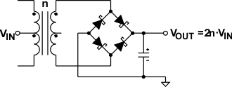
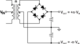
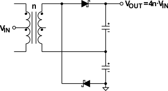
The device can drive push-pull converters that provide doubling output voltages, or bipolar outputs with different rectifier topologies . Figure 9-7 to Figure 9-9 show some of these topologies together with their respective open-circuit output voltages.
GUID-C8A1D3A3-0529-4CF8-9CE9-AC5603FF30D9-low.gif
Figure 9-7 Bridge Rectifier With Center-Tapped Secondary Enables Bipolar Outputs
GUID-46E7636D-DBB1-4EF1-AC32-B73A5598D286-low.gif
Figure 9-9 Half-Wave Rectifier Without Centered Ground and Center-Tapped Secondary Performs Voltage Doubling Twice, Hence Quadrupling VIN
GUID-C082A093-243F-4FA5-A14D-89E165434355-low.gif
Figure 9-8 Bridge Rectifier Without Center-Tapped Secondary Performs Voltage Doubling