ZHCSJ04D november   2018  – october 2020 SN6505A-Q1 , SN6505B-Q1 , SN6505D-Q1

PRODUCTION DATA  

  1.   1
  2. 特性
  3. 应用
  4. 说明
  5. Revision History
  6. Pin Configuration and Functions
  7. Specifications
    1. 6.1 Absolute Maximum Ratings
    2. 6.2 ESD Ratings
    3. 6.3 Recommended Operating Conditions
    4. 6.4 Thermal Information
    5. 6.5 Electrical Characteristics
    6. 6.6 Timing Requirements
    7. 6.7 Typical Characteristics, SN6505A-Q1
    8. 6.8 Typical Characteristics, SN6505B-Q1 or SN6505D-Q1
  8. Parameter Measurement Information
  9. Detailed Description
    1. 8.1 Overview
    2. 8.2 Functional Block Diagram
    3. 8.3 Feature Description
      1. 8.3.1 Push-Pull Converter
      2. 8.3.2 Core Magnetization
    4. 8.4 Device Functional Modes
      1. 8.4.1 Start-Up Mode
        1. 8.4.1.1 Soft-Start
      2. 8.4.2 Operating Mode
      3. 8.4.3 Shutdown-Mode
      4. 8.4.4 Spread Spectrum Clocking
      5. 8.4.5 External Clock Mode
  10. Application and Implementation
    1. 9.1 Application Information
    2. 9.2 Typical Application
      1. 9.2.1 Design Requirements
      2. 9.2.2 Detailed Design Procedure
        1. 9.2.2.1 Drive Capability
        2. 9.2.2.2 LDO Selection
        3. 9.2.2.3 Diode Selection
        4. 9.2.2.4 Capacitor Selection
        5. 9.2.2.5 Transformer Selection
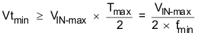
          1. 9.2.2.5.1 V-t Product Calculation
          2. 9.2.2.5.2 Turns Ratio Estimate
          3. 9.2.2.5.3 Recommended Transformers
      3. 9.2.3 Application Curves
      4. 9.2.4 System Examples
        1. 9.2.4.1 Higher Output Voltage Designs
        2. 9.2.4.2 Application Circuits
  11. 10Power Supply Recommendations
  12. 11Layout
    1. 11.1 Layout Guidelines
    2. 11.2 Layout Example
  13. 12Device and Documentation Support
    1. 12.1 Device Support
      1. 12.1.1 第三方产品免责声明
    2. 12.2 Documentation Support
      1. 12.2.1 Related Documentation
    3. 12.3 Related Links
    4. 12.4 接收文档更新通知
    5. 12.5 支持资源
    6. 12.6 Trademarks
    7. 12.7 静电放电警告
    8. 12.8 术语表
  14. 13Mechanical, Packaging, and Orderable Information

封装选项

机械数据 (封装 | 引脚)
散热焊盘机械数据 (封装 | 引脚)
订购信息
V-t Product Calculation

To prevent a transformer from saturation its V-t product must be greater than the maximum V-t product applied by the device. The maximum voltage delivered by the device is the nominal converter input plus 10%. The maximum time this voltage is applied to the primary is half the period of the lowest frequency at the specified input voltage. Therefore, the transformer’s minimum V-t product is determined through:

Equation 3. GUID-346F4E18-556C-40B4-9346-86CEF1F2096B-low.gif

Taking an example of fmin as 138 kHz for SN6505A-Q1 and 363 kHZ for SN6505B-Q1 or SN6505D-Q1 with a 5 V supply, Equation 3 yields the minimum V-t products of:

Equation 4. GUID-EA413FDB-59B1-4DAC-9295-6A96C102FE3E-low.gif

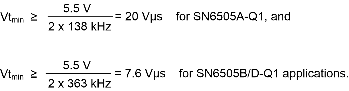
Common V-t values for low-power center-tapped transformers range from 22 Vμs to 150 Vμs with typical footprints of 10 mm x 12 mm. However, transformers specifically designed for PCMCIA applications provide as little as 11 Vμs and come with a significantly reduced footprint of 6 mm x 6 mm only.

While Vt-wise all of these transformers can be driven by the device, other important factors such as isolation voltage, transformer wattage, and turns ratio must be considered before making the final decision.