ZHCSV37T January 1993 – May 2024 SN54LVC00A , SN74LVC00A
PRODUCTION DATA
- 1
- 1 特性
- 2 应用
- 3 说明
- 4 Pin Configuration and Functions
-
5 Specifications
- 5.1 Absolute Maximum Ratings
- 5.2 ESD Ratings
- 5.3 Recommended Operating Conditions, SN54LVC00A
- 5.4 Recommended Operating Conditions, SN74LVC00A
- 5.5 Thermal Information
- 5.6 Electrical Characteristics, SN54LVC00A
- 5.7 Electrical Characteristics, SN74LVC00A
- 5.8 Switching Characteristics, SN54LVC00A
- 5.9 Switching Characteristics, SN74LVC00A
- 5.10 Operating Characteristics
- 5.11 Typical Characteristics
- 6 Parameter Measurement Information
- 7 Detailed Description
- 8 Application and Implementation
- 9 Device and Documentation Support
- 1046
- 11Mechanical, Packaging, and Orderable Information
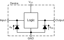
7.3.3 Clamp Diodes
The inputs and outputs to this device have negative clamping diodes.
CAUTION:
Voltages beyond the values specified in the Section 5.1 table can cause damage to the device. The input negative-voltage and output voltage ratings may be exceeded if the input and output clamp-current ratings are observed.
 Figure 7-2 Electrical Placement of Clamping Diodes for Each Input and Output