ZHCSDI7A December 2012 – March 2015 SM74611
PRODUCTION DATA.
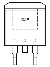
5 Pin Configuration and Functions
DDPAK
3 Pin (KTT)
Top View

Pin Functions
| PIN | I/O | DESCRIPTION | |
|---|---|---|---|
| NAME | NO. | ||
| ANODE | 1,3(1) | I | Connect both of these pins to the negative side of the PV cells |
| CATHODE | 2,DAP(2) | O | Pin 2 and the DAP are shorted internally. Connect the DAP to the positive side of the PV cells |
(1) Pin 1 and Pin 3 should be connected together for proper operation
(2) Package drawing at the end of datasheet is shown without Pin 2 being trimmed