ZHCSM80G October 2020 – September 2023 REF70
PRODMIX
- 1
- 1 特性
- 2 应用
- 3 说明
- 4 Revision History
- 5 Device Comparison Table
- 6 Pin Configuration and Functions
-
7 Specifications
- 7.1 Absolute Maximum Ratings
- 7.2 ESD Ratings
- 7.3 Recommended Operating Conditions
- 7.4 Thermal Information
- 7.5 REF7012 Electrical Characteristics
- 7.6 REF7025 Electrical Characteristics
- 7.7 REF7030 Electrical Characteristics
- 7.8 REF7033 Electrical Characteristics
- 7.9 REF7040 Electrical Characteristics
- 7.10 REF7050 Electrical Characteristics
- 7.11 Typical Characteristics
- 8 Parameter Measurement Information
- 9 Detailed Description
- 10Application and Implementation
- 11Device and Documentation Support
- 12Mechanical, Packaging, and Orderable Information
8.4.1 1/f Noise
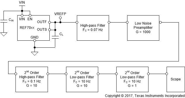
1/f noise, also known as flicker noise, is a low frequency noise that affects the device output voltage which can affect precision measurements in ADCs. This noise increases proportionally with output voltage and operating temperature. It is measured by filtering the output from 0.1-Hz to 10-Hz. Since the 1/f noise is an extremely low value, the frequency of interest needs to be amplified and band-pass filtered. This is done by using a high-pass filter to block the DC voltage. The resulting noise is then amplified by a gain of 1000. The bandpass filter is created by a series of high-pass and low-pass filter that adds additional gain to make it more visible on a oscilloscope as shown in Figure 8-9. 1/f noise must be tested in a Faraday cage enclosure to block environmental noise.
 Figure 8-9 1/f Noise Test Setup
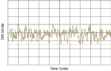
Typical 1/f noise (0.1-Hz to 10-Hz) distribution can be seen in Figure 8-10. The noise is measured at two different supply voltages. The REF70 noise performance is not impacted by supply voltage.
 Figure 8-10 0.1-Hz
to 10-Hz Voltage Noise Distribution
 Figure 8-11 0.1-Hz
to 10-Hz Voltage Noise