ZHCSPD4A April 2022 – September 2022 PCM3120-Q1
PRODUCTION DATA
- 1 特性
- 2 应用
- 3 说明
- 4 Revision History
- 5 Device Comparison Table
- 6 Pin Configuration and Functions
-
7 Specifications
- 7.1 Absolute Maximum Ratings
- 7.2 ESD Ratings
- 7.3 Recommended Operating Conditions
- Thermal Information
- 7.4 Electrical Characteristics
- 7.5 Timing Requirements: I2C Interface
- 7.6 Switching Characteristics: I2C Interface
- 7.7 Timing Requirements: TDM, I2S or LJ Interface
- 7.8 Switching Characteristics: TDM, I2S or LJ Interface
- Timing Requirements: PDM Digital Microphone Interface
- 7.9 Switching Characteristics: PDM Digial Microphone Interface
- 7.10 Timing Diagrams
- 7.11 Typical Characteristics
-
8 Detailed Description
- 8.1 Overview
- 8.2 Functional Block Diagram
- 8.3
Feature Description
- 8.3.1 Serial Interfaces
- 8.3.2 Phase-Locked Loop (PLL) and Clock Generation
- 8.3.3 Input Channel Configurations
- 8.3.4 Reference Voltage
- 8.3.5 Programmable Microphone Bias
- 8.3.6
Signal-Chain Processing
- 8.3.6.1 Programmable Channel Gain and Digital Volume Control
- 8.3.6.2 Programmable Channel Gain Calibration
- 8.3.6.3 Programmable Channel Phase Calibration
- 8.3.6.4 Programmable Digital High-Pass Filter
- 8.3.6.5 Programmable Digital Biquad Filters
- 8.3.6.6 Programmable Channel Summer and Digital Mixer
- 8.3.6.7
Configurable Digital Decimation Filters
- 8.3.6.7.1
Linear Phase Filters
- 8.3.6.7.1.1 Sampling Rate: 7.35 kHz to 8 kHz
- 8.3.6.7.1.2 Sampling Rate: 14.7 kHz to 16 kHz
- 8.3.6.7.1.3 Sampling Rate: 22.05 kHz to 24 kHz
- 8.3.6.7.1.4 Sampling Rate: 29.4 kHz to 32 kHz
- 8.3.6.7.1.5 Sampling Rate: 44.1 kHz to 48 kHz
- 8.3.6.7.1.6 Sampling Rate: 88.2 kHz to 96 kHz
- 8.3.6.7.1.7 Sampling Rate: 176.4 kHz to 192 kHz
- 8.3.6.7.1.8 Sampling Rate: 352.8 kHz to 384 kHz
- 8.3.6.7.1.9 Sampling Rate: 705.6 kHz to 768 kHz
- 8.3.6.7.2 Low-Latency Filters
- 8.3.6.7.3
Ultra-Low Latency Filters
- 8.3.6.7.3.1 Sampling Rate: 14.7 kHz to 16 kHz
- 8.3.6.7.3.2 Sampling Rate: 22.05 kHz to 24 kHz
- 8.3.6.7.3.3 Sampling Rate: 29.4 kHz to 32 kHz
- 8.3.6.7.3.4 Sampling Rate: 44.1 kHz to 48 kHz
- 8.3.6.7.3.5 Sampling Rate: 88.2 kHz to 96 kHz
- 8.3.6.7.3.6 Sampling Rate: 176.4 kHz to 192 kHz
- 8.3.6.7.3.7 Sampling Rate: 352.8 kHz to 384 kHz
- 8.3.6.7.1
Linear Phase Filters
- 8.3.7 Automatic Gain Controller (AGC)
- 8.3.8 Voice Activity Detection (VAD)
- 8.3.9 Digital PDM Microphone Record Channel
- 8.3.10 Interrupts, Status, and Digital I/O Pin Multiplexing
- 8.4 Device Functional Modes
- 8.5 Programming
- 8.6 Register Maps
- 9 Application and Implementation
- 10Power Supply Recommendations
- 11Layout
- 12Device and Documentation Support
- 13Mechanical, Packaging, and Orderable Information
8.3.3 Input Channel Configurations
The device consists of two pairs of analog input pins (INxP and INxM) that can be configured as differential inputs or single-ended inputs for the recording channel. The device supports simultaneous recording of up to two channels using the high-performance multichannel ADC. The input source for the analog pins can be from electret condenser analog microphones, micro-electro-mechanical system (MEMS) analog microphones, or line-in (auxiliary) inputs from the system board. Additionally, if the application uses digital PDM microphones for the recording, then the IN2P_GPI1, IN2M_GPO1, GPIO1, and MICBIAS_GPI2 pins can be reconfigured in the device to support up to four channels for the digital microphone recording. The device can also support simultaneous recording on two analog and two digital microphone channels. Table 8-8 shows the input source selection for the record channel.
| P0_R60_D[6:5] : CH1_INSRC[1:0] | INPUT CHANNEL 1 RECORD SOURCE SELECTION |
|---|---|
| 00 (default) | Analog differential input for channel 1 (this setting is valid only when the GPI1 and GPO1 pin functions are disabled) |
| 01 | Analog single-ended input for channel 1 (this setting is valid only when the GPI1 and GPO1 pin functions are disabled) |
| 10 | Digital PDM input for channel 1 (configure the GPIx and GPOx pin accordingly for PDMDIN1 and PDMCLK) |
| 11 | Reserved (do not use this setting) |
Similarly, the input source selection setting for input channel 2, channel 3, and channel 4 can be configured using the CH2_INSRC[1:0] (P0_R65_D[6:5]), CH3_INSRC[1:0] (P0_R70_D[6:5]), and CH4_INSRC[1:0] (P0_R75_D[6:5]) register bits, respectively.
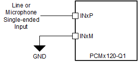
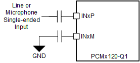
Typically, voice or audio signal inputs are capacitively coupled (AC coupled) to the device; however, the device also supports an option for DC-coupled inputs to save board space. This configuration can be done independently for each channel by setting the CH1_DC (P0_R60_D4), CH2_DC (P0_R65_D4), CH3_DC (P0_R70_D4), and CH4_DC (P0_R75_D4) register bits. The INxM pin can be directly grounded in DC-coupled mode (see Figure 8-14), but the INxM pin must be grounded after the AC-coupling capacitor in AC-coupled mode (see Figure 8-15) for the single-ended input configuration. For the best dynamic range performance, the differential AC-coupled input must be used .
 Figure 8-14 Single-Ended, DC-Coupled
Input Connection
 Figure 8-15 Single-Ended, AC-Coupled
Input Connection
Figure 8-15 Single-Ended, AC-Coupled
Input ConnectionThe device allows for flexibility in choosing the typical input impedance on INxP or INxM from 2.5 kΩ (default), 10 kΩ, and 20 kΩ based on the input source impedance. The higher input impedance results in slightly higher noise or lower dynamic range. Table 8-9 lists the configuration register settings for the input impedance for the record channel.
| P0_R60_D[3:2] : CH1_IMP[1:0] | CHANNEL 1 INPUT IMPEDANCE SELECTION |
|---|---|
| 00 (default) | Channel 1 input impedance typical value is 2.5 kΩ on INxP or INxM |
| 01 | Channel 1 input impedance typical value is 10 kΩ on INxP or INxM |
| 10 | Channel 1 input impedance typical value is 20 kΩ on INxP or INxM |
| 11 | Reserved (do not use this setting) |
Similarly, the input impedance selection setting for input channel 2 can be configured using the CH2_IMP[1:0] (P0_R65_D[3:2]) register bits.
The value of the coupling capacitor in AC-coupled mode must be chosen so that the high-pass filter formed by the coupling capacitor and the input impedance do not affect the signal content. Before proper recording can begin, this coupling capacitor must be charged up to the common-mode voltage at power up. To enable quick charging, the device has modes to speed up the charging of the coupling capacitor. The default value of the quick-charge timing is set for a coupling capacitor up to 1 µF. However, if a higher-value capacitor is used in the system, then the quick-charging timing can be increased by using the INCAP_QCHG (P0_R5_D[5:4]) register bits. For best distortion performance, use the low-voltage coefficient capacitors for AC coupling.
The PCM3120-Q1 can also support a higher input common-mode tolerance at the expense of noise performance by a few decibels. The device supports three different modes with different common-mode tolerances, which can be configured using the CH1_INP_CM_TOL_CFG[1:0] (P0_R58_D[7:6]) register bits. Table 8-10 lists the configuration register settings for the input impedance for the record channel.
| P0_R58_D[7:6] : CH1_INP_CM_TOL_CFG[1:0] | CHANNEL 1 INPUT COMMON-MODE TOLERANCE |
|---|---|
| 00 (default) | Channel 1 input common-mode tolerance of: AC-coupled input = 100 mVPP, DC-coupled input = 2.82 VPP. |
| 01 | Channel 1 input common-mode tolerance of: AC/DC-coupled input = 1 VPP. |
| 10 (high CMRR mode) | Channel 1 input common-mode tolerance of: AC/DC-coupled input = 0-AVDD (supported only with an input impedance of 10 kΩ and 20 kΩ). For input impedance of 2.5 kΩ, the input common-mode tolerance is 0.4 V to 2.6 V. |
| 11 | Reserved (do not use this setting) |
Similarly, the common-mode tolerance setting for input channel 2 can be configured using the CH2_INP_CM_TOL_CFG[1:0] (P0_R58_D[5:4]) register bits. See the Input Common Mode Tolerance and High CMRR modes for TLV320ADCx120 Devices application report for further details.