ZHCSQY6D august   2022  – april 2023 OPA2992-Q1 , OPA4992-Q1 , OPA992-Q1

PRODMIX  

  1. 特性
  2. 应用
  3. 说明
  4. Revision History
  5. Pin Configuration and Functions
  6. Specifications
    1. 6.1 Absolute Maximum Ratings
    2. 6.2 ESD Ratings
    3. 6.3 Recommended Operating Conditions
    4. 6.4 Thermal Information for Single Channel
    5. 6.5 Thermal Information for Dual Channel
    6. 6.6 Thermal Information for Quad Channel
    7. 6.7 Electrical Characteristics
    8. 6.8 Typical Characteristics
  7. Detailed Description
    1. 7.1 Overview
    2. 7.2 Functional Block Diagram
    3. 7.3 Feature Description
      1. 7.3.1 Input Protection Circuitry
      2. 7.3.2 EMI Rejection
      3. 7.3.3 Thermal Protection
      4. 7.3.4 Capacitive Load and Stability
      5. 7.3.5 Common-Mode Voltage Range
      6. 7.3.6 Phase Reversal Protection
      7. 7.3.7 Electrical Overstress
      8. 7.3.8 Overload Recovery
      9. 7.3.9 Typical Specifications and Distributions
    4. 7.4 Device Functional Modes
  8. Application and Implementation
    1. 8.1 Application Information
    2. 8.2 Typical Applications
      1. 8.2.1 Low-Side Current Measurement
        1. 8.2.1.1 Design Requirements
        2. 8.2.1.2 Detailed Design Procedure
        3. 8.2.1.3 Application Curve
    3. 8.3 Power Supply Recommendations
    4. 8.4 Layout
      1. 8.4.1 Layout Guidelines
      2. 8.4.2 Layout Example
  9. Device and Documentation Support
    1. 9.1 Device Support
      1. 9.1.1 Development Support
        1. 9.1.1.1 TINA-TI (Free Software Download)
    2. 9.2 Documentation Support
      1. 9.2.1 Related Documentation
    3. 9.3 接收文档更新通知
    4. 9.4 支持资源
    5. 9.5 Trademarks
    6. 9.6 静电放电警告
    7. 9.7 术语表
  10. 10Mechanical, Packaging, and Orderable Information

封装选项

机械数据 (封装 | 引脚)
散热焊盘机械数据 (封装 | 引脚)
订购信息

Common-Mode Voltage Range

The OPAx992-Q1 is a 40-V, true rail-to-rail input operational amplifier with an input common-mode range that extends to both supply rails. This wide range is achieved with paralleled complementary N-channel and P-channel differential input pairs, as shown in Figure 7-8. The N-channel pair is active for input voltages close to the positive rail, typically from (V+) – 1 V to the positive supply. The P-channel pair is active for inputs from the negative supply to approximately (V+) – 2 V. There is a small transition region, typically (V+) – 2 V to (V+) – 1 V, in which both input pairs are on. This transition region can vary modestly with process variation. Within this region PSRR, CMRR, offset voltage, offset drift, noise, and THD performance may be degraded compared to operation outside this region.

Figure 6-5 shows this transition region for a typical device in terms of input voltage offset in more detail.

For more information on common-mode voltage range and PMOS/NMOS pair interaction, see Op Amps With Complementary-Pair Input Stages application note.
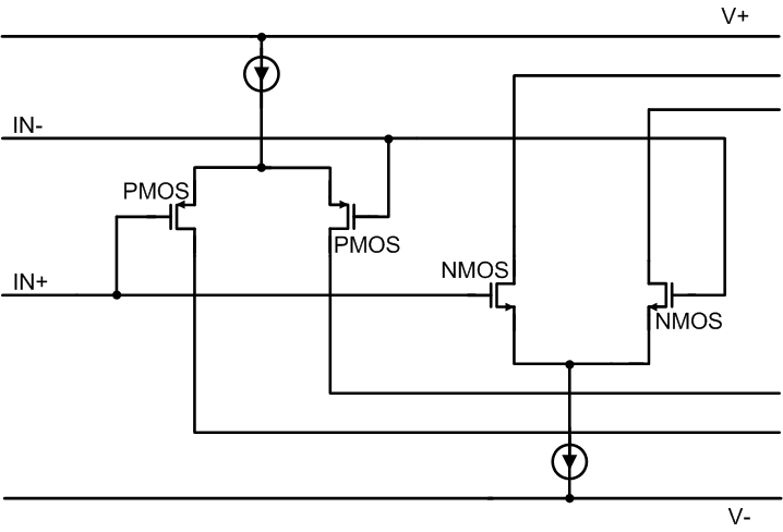
GUID-1018FB5C-B1A9-44C1-BB98-E82086BBED05-low.gifFigure 7-8 Rail-to-Rail Input Stage