ZHCSIQ9 September 2018 OPA859
PRODUCTION DATA.
9.4.2 Power-Down Mode
The OPA859 features a power-down mode to reduce the quiescent current to conserve power. Figure 23 and Figure 24 show the transient response of the OPA859 as the PD pin toggles between the disabled and enabled states.
The PD disable and enable threshold voltages are with reference to the negative supply. If the amplifier is configured with the positive supply at 3.3 V and the negative supply at ground, then the disable and enable threshold voltages are 0.65 V and 1.8 V, respectively. If the amplifier is configured with ±1.65-V supplies, then the disable and enable threshold voltages are at –1 V and 0.15 V, respectively. If the amplifier is configured with ±2.5-V supplies, then the threshold voltages are at –1.85 V and –0.7 V.
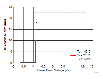
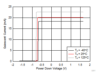
Figure 55 shows the switching behavior of a typical amplifier as the PD pin is swept down from the enabled state to the disabled state. Similarly, Figure 56 shows the switching behavior of a typical amplifier as the PD pin is swept up from the disabled state to the enabled state. The small difference in the switching thresholds between the down sweep and the up sweep is caused by the hysteresis designed into the amplifier to increase immunity to noise on the PD pin.
 Figure 55. Switching Threshold (PD Pin Swept from High to Low)
  Figure 56. Switching Threshold (PD Pin Swept from Low to High)
 Connecting the PD pin low disables the amplifier and places the output in a high-impedance state. When the amplifier is configured as a noninverting amplifier, the feedback (RF) and gain (RG) resistor network form a parallel load to the output of the amplifier. To protect the input stage of the amplifier, the OPA859 uses internal, back-to-back protection diodes between the inverting and noninverting input pins as Figure 49 shows. In the power-down state, if the differential voltage between the input pins of the amplifier exceeds a diode voltage drop, an additional low-impedance path is created between the noninverting input pin and the output pin.