ZHCSBX2D December 2013 – August 2016 OPA857
PRODUCTION DATA.
6 Specifications
6.1 Absolute Maximum Ratings(1)
over operating free-air temperature range (unless otherwise noted)| MIN | MAX | UNIT | ||
|---|---|---|---|---|
| Voltage | Supply voltage, VS– to VS+ | 3.8 | V | |
| Input and output voltage, VIN, VOUT pins | (VS–) – 0.7 | (VS+) + 0.7 | ||
| Differential input voltage | 1 | |||
| Current | Output current | 50 | mA | |
| Input current, VIN pin | 10 | |||
| Continuous power dissipation | See Thermal Information table | |||
| Temperature | Maximum junction, TJ | 150 | °C | |
| Maximum junction, TJ (continuous operation, long-term reliability) | 140 | |||
| Operating free-air, TA | –40 | 85 | ||
| Storage, Tstg | –65 | 150 | ||
(1) Stresses beyond those listed under absolute maximum ratings may cause permanent damage to the device. These are stress ratings only, and functional operation of the device at these or any other conditions beyond those indicated under recommended operating conditions is not implied. Exposure to absolute-maximum-rated conditions for extended periods may affect device reliability.
6.2 ESD Ratings
| VALUE | UNIT | |||
|---|---|---|---|---|
| V(ESD) | Electrostatic discharge | Human-body model (HBM), per ANSI/ESDA/JEDEC JS-001(1) | ±2000 | V |
| Charged-device model (CDM), per JEDEC specification JESD22-C101(2) | ±500 | |||
(1) JEDEC document JEP155 states that 500-V HBM allows safe manufacturing with a standard ESD control process.
(2) JEDEC document JEP157 states that 250-V CDM allows safe manufacturing with a standard ESD control process.
6.3 Recommended Operating Conditions
over operating free-air temperature range (unless otherwise noted)| MIN | NOM | MAX | UNIT | ||
|---|---|---|---|---|---|
| VSS | Supply input voltage | 2.7 | 3.3 | 3.6 | V |
| TJ | Operating junction temperature | –40 | 85 | °C | |
6.4 Thermal Information
| THERMAL METRIC(1) | OPA857 | UNIT | |
|---|---|---|---|
| RGT (VQFN) | |||
| 16 PINS | |||
| RθJA | Junction-to-ambient thermal resistance | 67.1 | °C/W |
| RθJC(top) | Junction-to-case(top) thermal resistance | 91.6 | °C/W |
| RθJB | Junction-to-board thermal resistance | 41.6 | °C/W |
| ψJT | Junction-to-top characterization parameter | 7.1 | °C/W |
| ψJB | Junction-to-board characterization parameter | 41.7 | °C/W |
| RθJC(bot) | Junction-to-case(bottom) thermal resistance | 23.1 | °C/W |
(1) For more information about traditional and new thermal metrics, see the Semiconductor and IC Package Thermal Metrics application report (SPRA953).
6.5 Electrical Characteristics
at TA = 25°C(2), VS = 3.3 V, VS+ – VS– = 3.3 V, CSource = 1.5 pF, VOUT = 0.5 VPP (differential), RL = 500-Ω differential, single-ended input, pseudo-differential output, and input and output referenced to midsupply (unless otherwise noted)| PARAMETER | TEST CONDITIONS | MIN | TYP | MAX | UNIT | TEST LEVEL(1) | |
|---|---|---|---|---|---|---|---|
| AC PERFORMANCE | |||||||
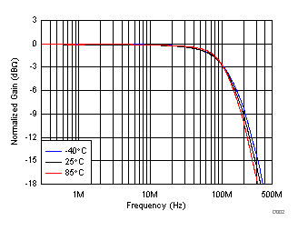
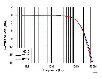
| Small-signal bandwidth | CTRL = 1, TA = –40°C to +85°C | 105 | MHz | C | |||
| CTRL = 0, TA = –40°C to +85°C | 125 | MHz | C | ||||
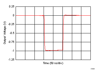
| SR | Slew rate (differential) | VOUT = 1-V step | 215 | V/μs | C | ||
| tS | Settling time to 1% | VOUT = 0.5-V step, CTRL = 0, TA = 25°C | 8 | ns | B | ||
| VOUT = 0.5-V step, CTRL = 1, TA = 25°C | 8 | ns | B | ||||
| Settling time to 0.001% | VOUT = 0.5-V step, CTRL = 0 | 600 | ns | C | |||
| VOUT = 0.5-V step, CTRL = 1 | 700 | ns | C | ||||
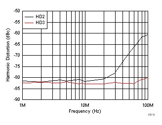
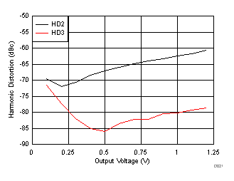
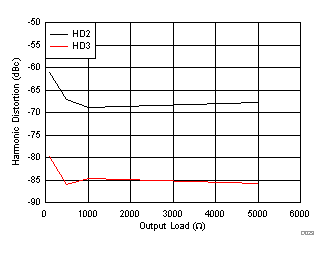
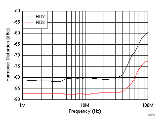
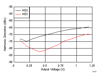
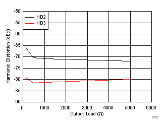
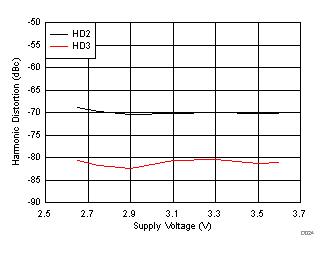
| HD2 | Second-harmonic distortion | VOUT = 0.5 VPP, f = 10 MHz, RF = 5 kΩ, TA = 25°C | –80 | dBc | C | ||
| VOUT = 0.5 VPP, f = 10 MHz, RF = 20 kΩ, TA = 25°C | –83 | dBc | C | ||||
| HD3 | Third-harmonic distortion | VOUT = 0.5 VPP, f = 10 MHz, RF = 5 kΩ, TA = 25°C | –88 | dBc | C | ||
| VOUT = 0.5 VPP, f = 10 MHz, RF = 20 kΩ, TA = 25°C | –83 | dBc | C | ||||
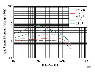
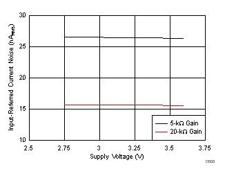
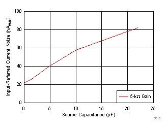
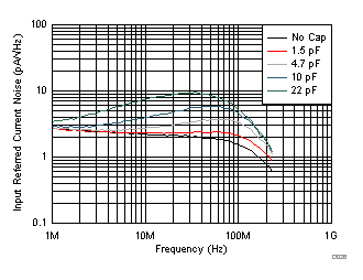
| Equivalent input-referred current noise | CTRL = 0, using 135-MHz brickwall filter | 25 | nARMS | C | |||
| CTRL = 1, using 135-MHz brickwall filter | 15 | nARMS | C | ||||
| Overdrive recovery time | IIN = 2x overload, CTRL = 1, settling to 1% of final value | 25 | ns | B | |||
| Closed-loop output impedance | f = 1 MHz (differential) | 50 | Ω | C | |||
| DC PERFORMANCE | |||||||
| Transimpedance gain | CTRL = 1 into 500 Ω(4)(5) | 18.2 | kΩ | C | |||
| CTRL = 0 into 500 Ω(4)(5) | 4.5 | kΩ | C | ||||
| Transimpedance gain error | TA = 25°C, RF = 20 kΩ and RF = 5 kΩ | ±1% | ±15% | A | |||
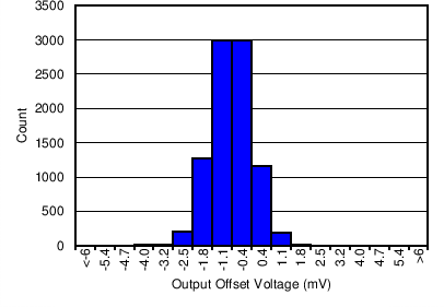
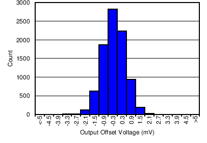
| VOO | Output offset voltage | TA = +25°C | ±1 | ±5 | mV | A | |
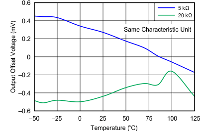
| TA = –40°C to +85°C(3) | ±6 | mV | B | ||||
| Output offset voltage drift | TA = –40°C to +85°C(3) | ±15 | μV/°C | C | |||
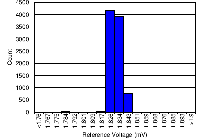
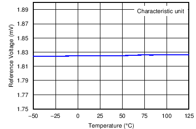
| VICR | Common-mode voltage range | TA = 25°C, OUTN | 1.78 | 1.83 | 1.88 | V | A |
| INPUT | |||||||
| Input pin capacitance | 2 | pF | C | ||||
| OUTPUT | |||||||
| Output voltage swing | OUT, TA = 25°C | 0.6 | 1.9 | V | A | ||
| TA = –40°C to +85°C(3) | 1.9 | V | B | ||||
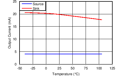
| Output current drive (for linear operation) |
OUT, differential 50-Ω between OUT and OUTN | +5 | mA | C | |||
| –20 | mA | C | |||||
| POWER SUPPLY | |||||||
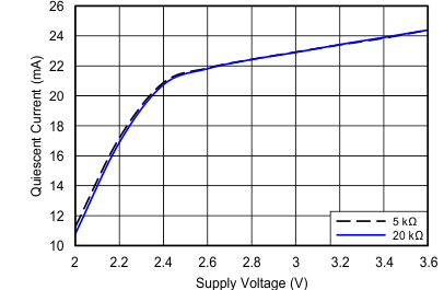
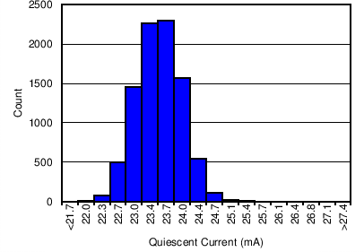
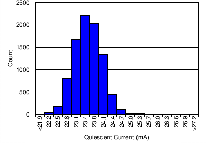
| Quiescent operating current | CTRL = 0, TA = 25°C | 20.5 | 23.4 | 26.3 | mA | A | |
| CTRL = 0, TA = –40°C to +85°C(3) | 20.0 | 26.8 | mA | B | |||
| CTRL = 1, TA = 25°C | 20.5 | 23.4 | 26.3 | mA | A | ||
| CTRL = 1, TA = –40°C to +85°C(3) | 20.0 | 26.8 | mA | B | |||
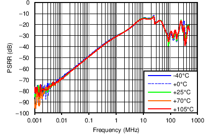
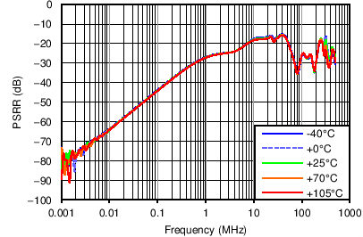
| PSRR | Power-supply rejection ratio | At dc, TA = 25°C | 70 | 80 | dB | A | |
| f = 10 MHz, TA = –40°C to +85°C(3) | 15 | 18 | dB | B | |||
| LOGIC LEVEL (CTRL) | |||||||
| VIH | High-level input voltage | 2 | V | A | |||
| VIL | Low-level input voltage | 0.8 | V | A | |||
| High-level control pin input bias current | 1 | µA | A | ||||
| Low-level control pin input bias current | 1 | µA | A | ||||
(1) Test levels: (A) 100% tested at 25°C. Overtemperature limits set by characterization and simulation. (B) Limits set by characterization and simulation. (C) Typical value only for information.
(2) Junction temperature = ambient for 70°C specifications.
(3) Junction temperature = ambient at low temperature; junction temperature = ambient + 3.5°C for overtemperature specifications.
(4) See the Application and Implementation section for details on loading and effective transimpedance gain.
(5) Note that the effective transimpedance gain is reduced to 18.2 kΩ and 4.5 kΩ, respectively, with a 500-Ω load resulting from the internal series resistance on OUT and OUTN.
6.6 Typical Characteristics
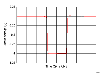
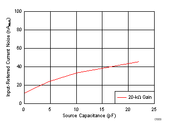
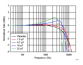
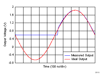
At TA = 25°C, CS = 1.5 pF, and RL = 500-Ω differential between OUT and OUTN (unless otherwise noted).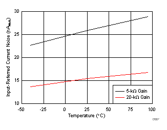
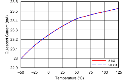
vs Temperature
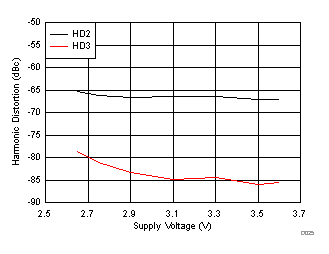
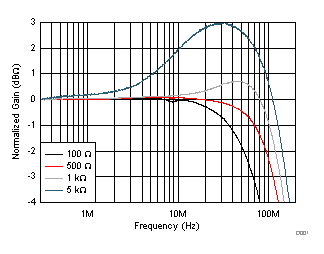
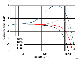
| TZ Gain = 20 kΩ, TA = 25°C, RLOAD = 500 Ω, f = 50 MHz | ||
