ZHCSF85A July   2016  – December 2019 OPA2626

PRODUCTION DATA.  

  1. 特性
  2. 应用
  3. 说明
    1.     Device Images
      1.      SAR ADC 驱动器
      2.      高保真拓扑改善了动态性能 (fIN = 10kHz,1MSPS FFT)
  4. 修订历史记录
  5. Pin Configuration and Functions
    1.     Pin Functions: OPA2626
  6. Specifications
    1. 6.1 Absolute Maximum Ratings
    2. 6.2 ESD Ratings
    3. 6.3 Recommended Operating Conditions
    4. 6.4 Thermal Information
    5. 6.5 Electrical Characteristics: High-Supply
    6. 6.6 Electrical Characteristics: Low-Supply
    7. 6.7 Typical Characteristics
  7. Parameter Measurement Information
    1. 7.1 DC Parameter Measurements
    2. 7.2 Transient Parameter Measurements
    3. 7.3 AC Parameter Measurements
    4. 7.4 Noise Parameter Measurements
  8. Detailed Description
    1. 8.1 Overview
    2. 8.2 Functional Block Diagram
    3. 8.3 Feature Description
      1. 8.3.1 SAR ADC Driver
      2. 8.3.2 Electrical Overstress
    4. 8.4 Device Functional Modes
      1. 8.4.1 High-Drive Mode
  9. Application and Implementation
    1. 9.1 Application Information
    2. 9.2 Typical Applications
      1. 9.2.1 Single-Supply, 16-Bit, 1-MSPS SAR ADC Driver
        1. 9.2.1.1 Design Requirements
        2. 9.2.1.2 Detailed Design Procedure
        3. 9.2.1.3 Application Curve
      2. 9.2.2 Single-Supply, 16-Bit, 1-MSPS, Multiplexed, SAR ADC Driver
        1. 9.2.2.1 Design Requirements
        2. 9.2.2.2 Detailed Design Procedure
        3. 9.2.2.3 Application Curves
  10. 10Power Supply Recommendations
  11. 11Layout
    1. 11.1 Layout Guidelines
    2. 11.2 Layout Example
  12. 12器件和文档支持
    1. 12.1 器件支持
      1. 12.1.1 开发支持
        1. 12.1.1.1 TINA-TI(免费软件下载)
        2. 12.1.1.2 TI 高精度设计
    2. 12.2 文档支持
      1. 12.2.1 相关文档
    3. 12.3 接收文档更新通知
    4. 12.4 社区资源
    5. 12.5 商标
    6. 12.6 静电放电警告
    7. 12.7 Glossary
  13. 13机械、封装和可订购信息

封装选项

机械数据 (封装 | 引脚)
散热焊盘机械数据 (封装 | 引脚)
订购信息

Design Requirements

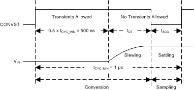
To optimize this circuit for performance, this design does not allow any large signal input transients at the driver circuit inputs for a small quiet-time period (tQT) towards the end of the previous conversion. The input step voltage can appear anytime from the beginning of conversion (CONVST rising edge) until the elapse of a half cycle time (0.5 × tCYC). This timing constraint on the input step allows a minimum settling time of (tQT + tACQ) for the ADC input to settle within the required accuracy, in the worst-case scenario. tQT + tACQ is the total time in which the output of the amplifier has to slew and settle within the required accuracy before the next conversion starts. Figure 65 shows this timing sequence.
OPA2626 Typ_App_Tim_SBO688.gifFigure 65. Timing Diagram for Input Signals