ZHCSFL2D October 2016 – June 2019 OPA2325 , OPA325 , OPA4325
PRODUCTION DATA.
8.2.2 Detailed Design Procedure
Traditional CMOS rail-to-rail input amplifiers use a complementary input stage: an N-channel input differential pair in parallel with a P-channel differential pair, as shown in Figure 47.
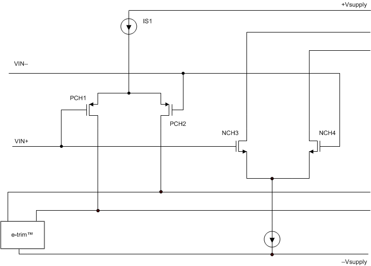 Figure 47. Complementary Input Stage (Traditional Rail-to-Rail Input CMOS Amplifiers)
 The N-channel pair is active for input voltages close to the positive rail, typically (V+) – 1 V to 200 mV above the positive supply, and the P-channel pair is on for inputs from 200 mV below the negative supply to approximately (V+) – 1 V. There is a small transition region, typically (V+) – 1.1 V to (V+) – 0.9 V, in which both pairs are on. This transition region is shown in Figure 48 for a traditional rail-to-rail input CMOS amplifier. Within this transition region, PSRR, CMRR, offset voltage, offset drift, and THD can be degraded when compared to device operation outside of this region.
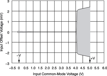 Figure 48. Input Offset Voltage vs Common-Mode Voltage
(For Traditional Rail-to-Rail Input CMOS Amplifiers)
The OPAx325 amplifiers include an internal charge pump that powers the amplifier input stage with an internal supply rail that is higher than the external power supply. The internal supply rail allows a single differential pair to operate and to be linear across the entire input common-mode voltage range, as shown in Figure 49.
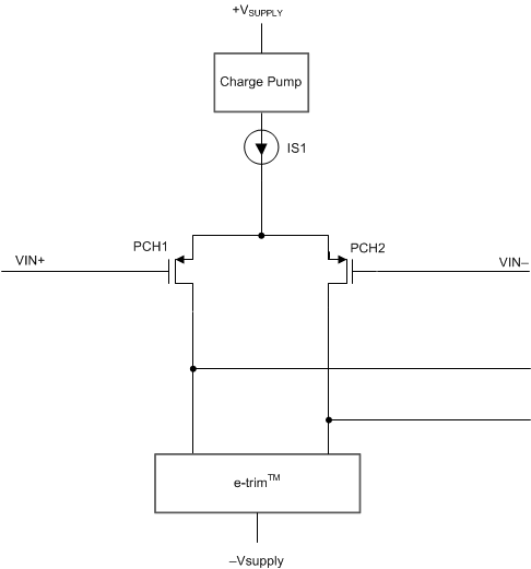 Figure 49. Single Differential Input Pair with a Charge Pump (Zero-Crossover)
 The unique zero-crossover topology shown in Figure 49 eliminates the input offset transition region, typical of most rail-to-rail input operational amplifiers. This topology allows the OPAx325 to provide superior CMRR across the entire common-mode input range that extends 100 mV beyond both power-supply rails. Figure 50 shows the input offset voltage versus input common-mode voltage plot for the OPAx325.
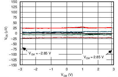 Figure 50. Offset Voltage vs Common-Mode Voltage (OPAx325, Zero-Crossover Amplifier)
 The OPAx325 and a typical CMOS amplifier were used in identical circuits where these amplifiers were configured as a unity-gain buffer amplifier; see Figure 51 and Figure 52. A pure sine wave with an amplitude of 2 V (4 VPP) was given as input to the two identical circuits of Figure 51 and Figure 52. The outputs of these circuits were captured on a spectrum analyzer. Figure 53 and Figure 54 illustrate the output voltage spectrum for the OPAx325 and a typical CMOS rail-to-rail amplifier, respectively. The output of the OPAx325 has very few spurs and harmonics when compared to the typical rail-to-rail CMOS amplifier, as illustrated in Figure 55.
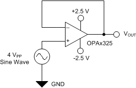 Figure 51. OPAx325 as a Unity-Gain Buffer
 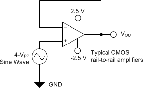 Figure 52. Typical CMOS Rail-to-Rail Amplifier as a Unity-Gain Buffer