ZHCSGC1F June 2017 – March 2021 OPA145 , OPA2145
PRODUCTION DATA
- 1 特性
- 2 应用
- 3 说明
- 4 Revision History
- 5 Pin Configuration and Functions
- 6 Specifications
- 7 Detailed Description
- 8 Application and Implementation
- 9 Power Supply Recommendations
- 10Layout
- 11Device and Documentation Support
- 12Mechanical, Packaging, and Orderable Information
7.3.3 Noise Performance
Figure 7-1 shows the total circuit noise for varying source impedances with the operational amplifier in a unity-gain configuration (with no feedback resistor network and therefore no additional noise contributions). The OPAx145 and OPAx211 are shown with total circuit noise calculated. The op amp contributes both a voltage noise component and a current noise component. The voltage noise is commonly modeled as a time-varying component of the offset voltage. The current noise is modeled as the time-varying component of the input bias current and reacts with the source resistance to create a voltage component of noise. Therefore, the lowest noise op amp for a given application depends on the source impedance. For low source impedance, current noise is negligible, and voltage noise generally dominates. The OPAx145 has both low voltage noise and extremely low current noise because of the FET input of the op amp. As a result, the current noise contribution of the OPAx145 is negligible for any practical source impedance, which makes it the better choice for applications with high source impedance.

Equation 1 can be used to calculate the total noise at the output of the amplifier. A plot can be created using this equation to quickly compare the noise performance of two different amplifiers when used with different source resistances, as is shown in Figure 7-1.
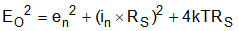
- en = voltage noise
- In = current noise
- RS = source impedance
- k = Boltzmann's constant = 1.38 × 10⁻²³ J/K
- T = temperature in kelvins (K)
For more details on calculating noise, see Section 7.3.4.