ZHCSJH0C March   2019  – September 2022 OPA1655 , OPA1656

PRODUCTION DATA  

  1. 特性
  2. 应用
  3. 说明
  4. Revision History
  5. Pin Configuration and Functions
  6. Specifications
    1. 6.1 Absolute Maximum Ratings
    2. 6.2 ESD Ratings
    3. 6.3 Recommended Operating Conditions
    4. 6.4 Thermal Information: OPA1655
    5. 6.5 Thermal Information: OPA1656
    6. 6.6 Electrical Characteristics
    7. 6.7 Typical Characteristics
  7. Detailed Description
    1. 7.1 Overview
    2. 7.2 Functional Block Diagram
    3. 7.3 Feature Description
      1. 7.3.1 Phase Reversal Protection
      2. 7.3.2 Electrical Overstress
      3. 7.3.3 EMI Rejection Ratio (EMIRR)
        1. 7.3.3.1 EMIRR IN+ Test Configuration
    4. 7.4 Device Functional Modes
  8. Application and Implementation
    1. 8.1 Application Information
      1. 8.1.1 Basic Noise Calculations
    2. 8.2 Typical Applications
      1. 8.2.1 Preamplifier Circuit for Vinyl Record Playback With Moving-Magnet Phono Cartridges
        1. 8.2.1.1 Design Requirements
        2. 8.2.1.2 Detailed Design Procedure
        3. 8.2.1.3 Application Curves
      2. 8.2.2 Composite Headphone Amplifier
        1. 8.2.2.1 Application Curves
      3. 8.2.3 Baxandall Tone Control
        1. 8.2.3.1 Application Curves
      4. 8.2.4 Guitar Input to XLR Output
        1. 8.2.4.1 Application Curves
    3. 8.3 Power Supply Recommendations
    4. 8.4 Layout
      1. 8.4.1 Layout Guidelines
        1. 8.4.1.1 Power Dissipation
      2. 8.4.2 Layout Example
  9. Device and Documentation Support
    1. 9.1 Device Support
      1. 9.1.1 Development Support
        1. 9.1.1.1 PSpice® for TI
        2. 9.1.1.2 TINA-TI™ Simulation Software (Free Download)
        3. 9.1.1.3 DIP-Adapter-EVM
        4. 9.1.1.4 DIYAMP-EVM
        5. 9.1.1.5 TI Reference Designs
        6. 9.1.1.6 Filter Design Tool
    2. 9.2 Documentation Support
      1. 9.2.1 Related Documentation
    3. 9.3 接收文档更新通知
    4. 9.4 支持资源
    5. 9.5 Trademarks
    6. 9.6 Electrostatic Discharge Caution
    7. 9.7 术语表
  10. 10Mechanical, Packaging, and Orderable Information

封装选项

机械数据 (封装 | 引脚)
散热焊盘机械数据 (封装 | 引脚)
订购信息

Basic Noise Calculations

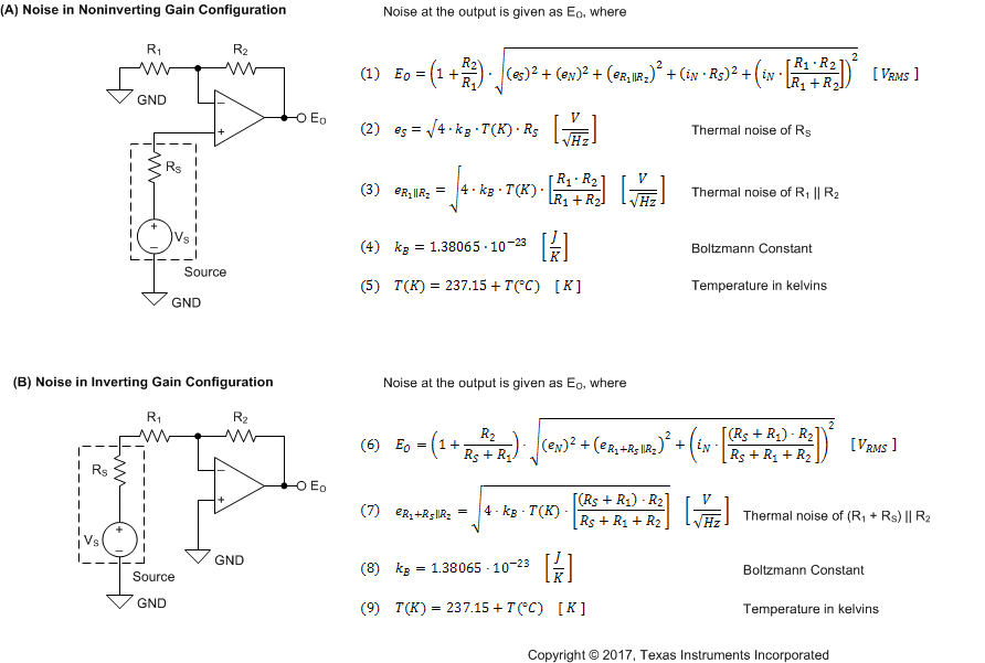
Low-noise circuit design requires careful analysis of all noise sources. External noise sources can dominate in many cases; consider the effect of source resistance on overall op amp noise performance. Total noise of the circuit is the root-sum-square combination of all noise components.

Figure 8-1 shows noninverting (A) and inverting (B) op amp circuit configurations with gain. In circuit configurations with gain, the feedback network resistors contribute noise. In general, the current noise of the op amp reacts with the feedback resistors to create additional noise components.

The selected feedback resistor values make these noise sources negligible. Low impedance feedback resistors load the output of the amplifier. The equations for total noise are shown for both configurations.
GUID-09CAC1F2-BB46-43E8-B9AE-285BB2BDA145-low.gif

where

  • eN is the voltage noise of the amplifier. For the OPA165x, eN = 4.3 nV/√Hz at 1 kHz.
  • iN is the current noise of the amplifier. For the OPA165x, iN = 6 fA/√Hz at 1 kHz.
Note: For additional resources on noise calculations, see TI's Precision Labs Series.
Figure 8-1 Noise Calculation in Gain Configurations