ZHCS474F August 2010 – September 2019 MSP430F5324 , MSP430F5325 , MSP430F5326 , MSP430F5327 , MSP430F5328 , MSP430F5329
PRODUCTION DATA.
- 1器件概述
- 2修订历史记录
- 3Device Comparison
- 4Terminal Configuration and Functions
-
5Specifications
- 5.1 Absolute Maximum Ratings
- 5.2 ESD Ratings
- 5.3 Recommended Operating Conditions
- 5.4 Active Mode Supply Current Into VCC Excluding External Current
- 5.5 Low-Power Mode Supply Currents (Into VCC) Excluding External Current
- 5.6 Thermal Resistance Characteristics
- 5.7 Schmitt-Trigger Inputs – General-Purpose I/O (P1.0 to P1.7, P2.0 to P2.7, P3.0 to P3.7, P4.0 to P4.7) (P5.0 to P5.7, P6.0 to P6.7, P7.0 to P7.7, P8.0 to P8.2, PJ.0 to PJ.3, RST/NMI)
- 5.8 Inputs – Ports P1 and P2 (P1.0 to P1.7, P2.0 to P2.7)
- 5.9 Leakage Current – General-Purpose I/O (P1.0 to P1.7, P2.0 to P2.7, P3.0 to P3.7, P4.0 to P4.7) (P5.0 to P5.7, P6.0 to P6.7, P7.0 to P7.7, P8.0 to P8.2, PJ.0 to PJ.3, RST/NMI)
- 5.10 Outputs – General-Purpose I/O (Full Drive Strength) (P1.0 to P1.7, P2.0 to P2.7, P3.0 to P3.7, P4.0 to P4.7) (P5.0 to P5.7, P6.0 to P6.7, P7.0 to P7.7, P8.0 to P8.2, PJ.0 to PJ.3)
- 5.11 Outputs – General-Purpose I/O (Reduced Drive Strength) (P1.0 to P1.7, P2.0 to P2.7, P3.0 to P3.7, P4.0 to P4.7) (P5.0 to P5.7, P6.0 to P6.7, P7.0 to P7.7, P8.0 to P8.2, PJ.0 to PJ.3)
- 5.12 Output Frequency – General-Purpose I/O (P1.0 to P1.7, P2.0 to P2.7, P3.0 to P3.7, P4.0 to P4.7) (P5.0 to P5.7, P6.0 to P6.7, P7.0 to P7.7, P8.0 to P8.2, PJ.0 to PJ.3)
- 5.13 Typical Characteristics – Outputs, Reduced Drive Strength (PxDS.y = 0)
- 5.14 Typical Characteristics – Outputs, Full Drive Strength (PxDS.y = 1)
- 5.15 Crystal Oscillator, XT1, Low-Frequency Mode
- 5.16 Crystal Oscillator, XT2
- 5.17 Internal Very-Low-Power Low-Frequency Oscillator (VLO)
- 5.18 Internal Reference, Low-Frequency Oscillator (REFO)
- 5.19 DCO Frequency
- 5.20 PMM, Brownout Reset (BOR)
- 5.21 PMM, Core Voltage
- 5.22 PMM, SVS High Side
- 5.23 PMM, SVM High Side
- 5.24 PMM, SVS Low Side
- 5.25 PMM, SVM Low Side
- 5.26 Wake-up Times From Low-Power Modes and Reset
- 5.27 Timer_A
- 5.28 Timer_B
- 5.29 USCI (UART Mode) Clock Frequency
- 5.30 USCI (UART Mode)
- 5.31 USCI (SPI Master Mode) Clock Frequency
- 5.32 USCI (SPI Master Mode)
- 5.33 USCI (SPI Slave Mode)
- 5.34 USCI (I2C Mode)
- 5.35 12-Bit ADC, Power Supply and Input Range Conditions
- 5.36 12-Bit ADC, Timing Parameters
- 5.37 12-Bit ADC, Linearity Parameters Using an External Reference Voltage or AVCC as Reference Voltage
- 5.38 12-Bit ADC, Linearity Parameters Using the Internal Reference Voltage
- 5.39 12-Bit ADC, Temperature Sensor and Built-In VMID
- 5.40 REF, External Reference
- 5.41 REF, Built-In Reference
- 5.42 Comparator B
- 5.43 Ports PU.0 and PU.1
- 5.44 LDO-PWR (LDO Power System)
- 5.45 Flash Memory
- 5.46 JTAG and Spy-Bi-Wire Interface
-
6Detailed Description
- 6.1 CPU (Link to User's Guide)
- 6.2 Operating Modes
- 6.3 Interrupt Vector Addresses
- 6.4 Memory Organization
- 6.5 Bootloader (BSL)
- 6.6 JTAG Operation
- 6.7 Flash Memory (Link to User's Guide)
- 6.8 RAM (Link to User's Guide)
- 6.9
Peripherals
- 6.9.1 Digital I/O (Link to User's Guide)
- 6.9.2 Port Mapping Controller (Link to User's Guide)
- 6.9.3 Oscillator and System Clock (Link to User's Guide)
- 6.9.4 Power-Management Module (PMM) (Link to User's Guide)
- 6.9.5 Hardware Multiplier (MPY) (Link to User's Guide)
- 6.9.6 Real-Time Clock (RTC_A) (Link to User's Guide)
- 6.9.7 Watchdog Timer (WDT_A) (Link to User's Guide)
- 6.9.8 System Module (SYS) (Link to User's Guide)
- 6.9.9 DMA Controller (Link to User's Guide)
- 6.9.10 Universal Serial Communication Interface (USCI) (Links to User's Guide: UART Mode, SPI Mode, I2C Mode)
- 6.9.11 TA0 (Link to User's Guide)
- 6.9.12 TA1 (Link to User's Guide)
- 6.9.13 TA2 (Link to User's Guide)
- 6.9.14 TB0 (Link to User's Guide)
- 6.9.15 Comparator_B (Link to User's Guide)
- 6.9.16 ADC12_A (Link to User's Guide)
- 6.9.17 CRC16 (Link to User's Guide)
- 6.9.18 REF Voltage Reference (Link to User's Guide)
- 6.9.19 Embedded Emulation Module (EEM) (Link to User's Guide)
- 6.9.20 Peripheral File Map
- 6.10
Input/Output Diagrams
- 6.10.1 Port P1 (P1.0 to P1.7) Input/Output With Schmitt Trigger
- 6.10.2 Port P2 (P2.0 to P2.7) Input/Output With Schmitt Trigger
- 6.10.3 Port P3 (P3.0 to P3.7) Input/Output With Schmitt Trigger
- 6.10.4 Port P4 (P4.0 to P4.7) Input/Output With Schmitt Trigger
- 6.10.5 Port P5 (P5.0 and P5.1) Input/Output With Schmitt Trigger
- 6.10.6 Port P5 (P5.2) Input/Output With Schmitt Trigger
- 6.10.7 Port P5 (P5.3) Input/Output With Schmitt Trigger
- 6.10.8 Port P5 (P5.4 and P5.5) Input/Output With Schmitt Trigger
- 6.10.9 Port P5 (P5.6 to P5.7), Input/Output With Schmitt Trigger
- 6.10.10 Port P6 (P6.0 to P6.7) Input/Output With Schmitt Trigger
- 6.10.11 Port P7 (P7.0 to P7.3) Input/Output With Schmitt Trigger
- 6.10.12 Port P7 (P7.4 to P7.7) Input/Output With Schmitt Trigger
- 6.10.13 Port P8 (P8.0 to P8.2) Input/Output With Schmitt Trigger
- 6.10.14 Port U (PU.0 and PU.1)
- 6.10.15 Port J (PJ.0) JTAG Pin TDO, Input/Output With Schmitt Trigger or Output
- 6.10.16 Port J (PJ.1 to PJ.3) JTAG Pins TMS, TCK, TDI/TCLK, Input/Output With Schmitt Trigger or Output
- 6.11 Device Descriptors
- 7器件和文档支持
- 8机械、封装和可订购信息
4.1 Pin Diagrams
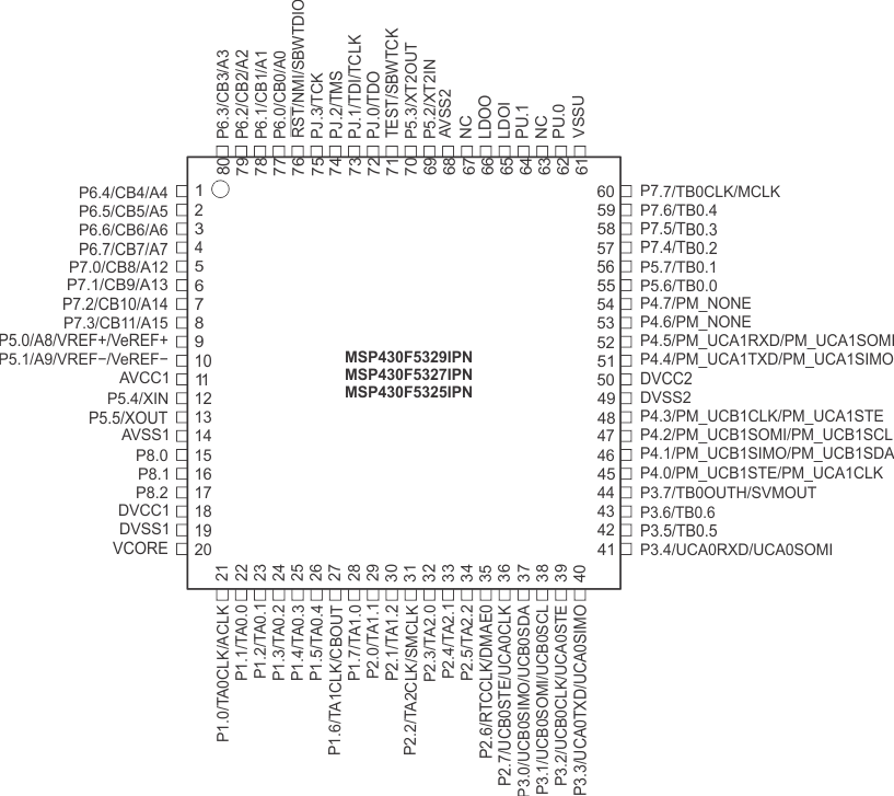
Figure 4-1 shows the pinout for the F5329, F5327, and F5325 devices in the 80-pin PN package.
 Figure 4-1 80-Pin PN Package (Top View) – MSP430F5329IPN, MSP430F5327IPN, MSP430F5325IPN
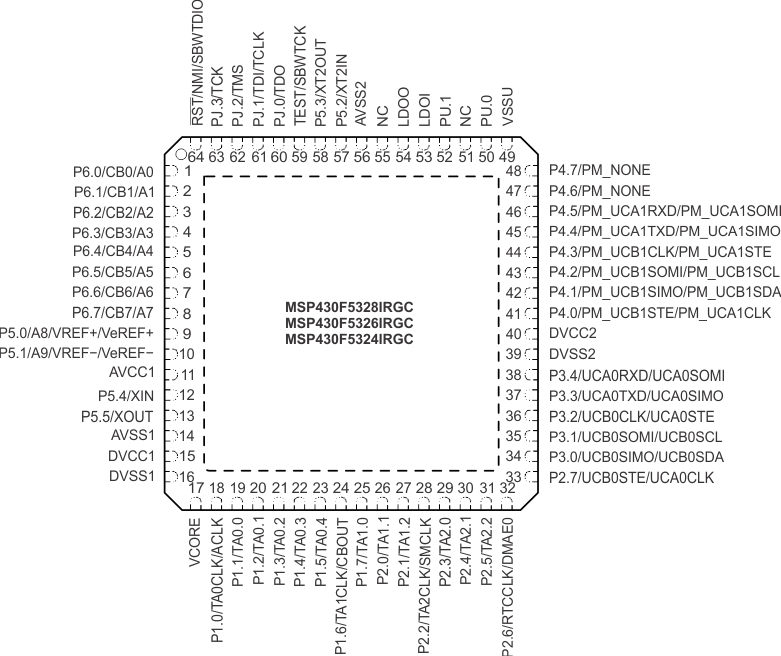
 Figure 4-2 shows the pinout for the F5328, F5326, and F5324 devices in the 64-pin RGC package.
 Figure 4-2 64-Pin RGC Package (Top View) – MSP430F5328IRGC, MSP430F5326IRGC, MSP430F5324IRGC
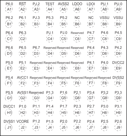
 Figure 4-3 shows the pinout for the F5328, F5326, and F5324 devices in the 80-pin ZQE package. This figure shows the default signal name for each pin; see Table 4-1 for additional signals.
