ZHCSAJ5H November 2012 – September 2018 MSP430F5212 , MSP430F5214 , MSP430F5217 , MSP430F5219 , MSP430F5222 , MSP430F5224 , MSP430F5229
PRODUCTION DATA.
- 1器件概述
- 2修订历史记录
- 3Device Comparison
- 4Terminal Configuration and Functions
-
5Specifications
- 5.1 Absolute Maximum Ratings
- 5.2 ESD Ratings
- 5.3 Recommended Operating Conditions
- 5.4 Active Mode Supply Current Into VCC Excluding External Current
- 5.5 Low-Power Mode Supply Currents (Into VCC) Excluding External Current
- 5.6 Thermal Resistance Characteristics
- 5.7 Schmitt-Trigger Inputs – General-Purpose I/O DVCC Domain (P1.0 to P1.3, P5.0 to P5.5, P6.0 to P6.7, PJ.0 to PJ.3, RSTDVCC)
- 5.8 Schmitt-Trigger Inputs – General-Purpose I/O DVIO Domain (P1.4 to P1.7, P2.0 to P2.7, P3.0 to P3.4, P4.0 to P4.7, P7.0 to P7.5, RST/NMI, BSLEN)
- 5.9 Inputs – Interrupts DVCC Domain Port P1 (P1.0 to P1.3)
- 5.10 Inputs – Interrupts DVIO Domain Ports P1 and P2 (P1.4 to P1.7, P2.0 to P2.7)
- 5.11 Leakage Current – General-Purpose I/O DVCC Domain (P1.0 to P1.3, P5.0 to P5.5, P6.0 to P6.7, PJ.0 to PJ.3)
- 5.12 Leakage Current – General-Purpose I/O DVIO Domain (P1.4 to P1.7, P2.0 to P2.7, P3.0 to P3.4, P4.0 to P4.7, P7.0 to P7.5)
- 5.13 Outputs – General-Purpose I/O DVCC Domain (Full Drive Strength) (P1.0 to P1.3, P5.0 to P5.5, P6.0 to P6.7, PJ.0 to PJ.3)
- 5.14 Outputs – General-Purpose I/O DVCC Domain (Reduced Drive Strength) (P1.0 to P1.3, P5.0 to P5.5, P6.0 to P6.7, PJ.0 to PJ.3)
- 5.15 Outputs – General-Purpose I/O DVIO Domain (Full Drive Strength) (P1.4 to P1.7, P2.0 to P2.7, P3.0 to P3.4, P4.0 to P4.7, P7.0 to P7.5)
- 5.16 Outputs – General-Purpose I/O DVIO Domain (Reduced Drive Strength) (P1.4 to P1.7, P2.0 to P2.7, P3.0 to P3.4, P4.0 to P4.7, P7.0 to P7.5)
- 5.17 Output Frequency – General-Purpose I/O DVCC Domain (P1.0 to P1.3, P5.0 to P5.5, P6.0 to P6.7, PJ.0 to PJ.3)
- 5.18 Output Frequency – General-Purpose I/O DVIO Domain (P1.4 to P1.7, P2.0 to P2.7, P3.0 to P3.4, P4.0 to P4.7, P7.0 to P7.5)
- 5.19 Typical Characteristics – Outputs, Reduced Drive Strength (PxDS.y = 0)
- 5.20 Typical Characteristics – Outputs, Full Drive Strength (PxDS.y = 1)
- 5.21 Crystal Oscillator, XT1, Low-Frequency Mode
- 5.22 Crystal Oscillator, XT2
- 5.23 Internal Very-Low-Power Low-Frequency Oscillator (VLO)
- 5.24 Internal Reference, Low-Frequency Oscillator (REFO)
- 5.25 DCO Frequency
- 5.26 PMM, Brownout Reset (BOR)
- 5.27 PMM, Core Voltage
- 5.28 PMM, SVS High Side
- 5.29 PMM, SVM High Side
- 5.30 PMM, SVS Low Side
- 5.31 PMM, SVM Low Side
- 5.32 Wake-up Times From Low-Power Modes and Reset
- 5.33 Timer_A
- 5.34 Timer_B
- 5.35 USCI (UART Mode), Recommended Operating Conditions
- 5.36 USCI (UART Mode)
- 5.37 USCI (SPI Master Mode), Recommended Operating Conditions
- 5.38 USCI (SPI Master Mode)
- 5.39 USCI (SPI Slave Mode)
- 5.40 USCI (I2C Mode)
- 5.41 10-Bit ADC, Power Supply and Input Range Conditions
- 5.42 10-Bit ADC, Timing Parameters
- 5.43 10-Bit ADC, Linearity Parameters
- 5.44 REF, External Reference
- 5.45 REF, Built-In Reference
- 5.46 Comparator_B
- 5.47 Flash Memory
- 5.48 JTAG and Spy-Bi-Wire Interface
- 5.49 DVIO BSL Entry
-
6Detailed Description
- 6.1 CPU (Link to user's guide)
- 6.2 Operating Modes
- 6.3 Interrupt Vector Addresses
- 6.4 Memory Organization
- 6.5 Bootloader (BSL)
- 6.6 JTAG Operation
- 6.7 Flash Memory (Link to user's guide)
- 6.8 RAM (Link to user's guide)
- 6.9
Peripherals
- 6.9.1 Digital I/O (Link to user's guide)
- 6.9.2 Port Mapping Controller (Link to user's guide)
- 6.9.3 Oscillator and System Clock (Link to user's guide)
- 6.9.4 Power-Management Module (PMM) (Link to user's guide)
- 6.9.5 Hardware Multiplier (Link to user's guide)
- 6.9.6 Real-Time Clock (RTC_A) (Link to user's guide)
- 6.9.7 Watchdog Timer (WDT_A) (Link to user's guide)
- 6.9.8 System Module (SYS) (Link to user's guide)
- 6.9.9 DMA Controller (Link to user's guide)
- 6.9.10 Universal Serial Communication Interface (USCI) (Links to user's guide: UART Mode, SPI Mode, I2C Mode)
- 6.9.11 TA0 (Link to user's guide)
- 6.9.12 TA1 (Link to user's guide)
- 6.9.13 TA2 (Link to user's guide)
- 6.9.14 TB0 (Link to user's guide)
- 6.9.15 Comparator_B (Link to user's guide)
- 6.9.16 ADC10_A (Link to user's guide)
- 6.9.17 CRC16 (Link to user's guide)
- 6.9.18 REF Voltage Reference (Link to user's guide)
- 6.9.19 Embedded Emulation Module (EEM) (S Version) (Link to user's guide)
- 6.9.20 Peripheral File Map
- 6.10
Input/Output Diagrams
- 6.10.1 Port P1 (P1.0 to P1.7) Input/Output With Schmitt Trigger
- 6.10.2 Port P2 (P2.0 to P2.7) Input/Output With Schmitt Trigger
- 6.10.3 Port P3 (P3.0 to P3.4) Input/Output With Schmitt Trigger
- 6.10.4 Port P4 (P4.0 to P4.7) Input/Output With Schmitt Trigger
- 6.10.5 Port P5 (P5.0 and P5.1) Input/Output With Schmitt Trigger
- 6.10.6 Port P5 (P5.2) Input/Output With Schmitt Trigger
- 6.10.7 Port P5 (P5.3) Input/Output With Schmitt Trigger
- 6.10.8 Port P5 (P5.4 and P5.5) Input/Output With Schmitt Trigger
- 6.10.9 Port P6 (P6.0 to P6.7) Input/Output With Schmitt Trigger
- 6.10.10 Port P7 (P7.0 to P7.5) Input/Output With Schmitt Trigger
- 6.10.11 Port PJ (PJ.0) JTAG Pin TDO, Input/Output With Schmitt Trigger or Output
- 6.10.12 Port PJ (PJ.1 to PJ.3) JTAG Pins TMS, TCK, TDI/TCLK, Input/Output With Schmitt Trigger or Output
- 6.11 Device Descriptors
- 7器件和文档支持
- 8机械、封装和可订购信息
5.3 Recommended Operating Conditions
| MIN | NOM | MAX | UNIT | |||
|---|---|---|---|---|---|---|
| VCC | Supply voltage during program execution and flash programming (AVCC = DVCC)(1)(3)(2) | PMMCOREVx = 0 | 1.8 | 3.6 | V | |
| PMMCOREVx = 0, 1 | 2.0 | 3.6 | ||||
| PMMCOREVx = 0, 1, 2 | 2.2 | 3.6 | ||||
| PMMCOREVx = 0, 1, 2, 3 | 2.4 | 3.6 | ||||
| VIO | Supply voltage applied to DVIO referenced to VSS(3) | 1.62 | 1.98 | V | ||
| VSS | Supply voltage (AVSS = DVSS) | 0 | V | |||
| TA | Operating free-air temperature | –40 | 85 | °C | ||
| TJ | Operating junction temperature | –40 | 85 | °C | ||
| CVCORE | Recommended capacitor at VCORE(4) | 470 | nF | |||
| CDVCC/ CVCORE | Capacitor ratio of DVCC to VCORE | 10 | ||||
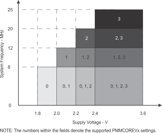
| fSYSTEM | Processor frequency (maximum MCLK frequency)(5) (see Figure 5-3) | PMMCOREVx = 0 (default condition),
1.8 V ≤ VCC ≤ 3.6 V |
0 | 8 | MHz | |
| PMMCOREVx = 1,
2.0 V ≤ VCC ≤ 3.6 V |
0 | 12 | ||||
| PMMCOREVx = 2,
2.2 V ≤ VCC ≤ 3.6 V |
0 | 20 | ||||
| PMMCOREVx = 3,
2.4 V ≤ VCC ≤ 3.6 V |
0 | 25 | ||||
(1) TI recommends powering AVCC and DVCC from the same source. A maximum difference of 0.3 V between AVCC and DVCC can be tolerated during power up and operation.
(2) The minimum supply voltage is defined by the supervisor SVS levels when it is enabled. See the Section 5.28 threshold parameters for the exact values and further details.
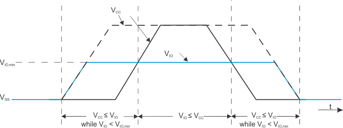
(3) During VCC and VIO power up, it is required that VIO ≥ VCC during the ramp up phase of VIO. During VCC and VIO power down, it is required that VIO ≥ VCC during the ramp down phase of VIO (see Figure 5-1).
(4) A capacitor tolerance of ±20% or better is required.
(5) Modules may have a different maximum input clock specification. See the specification of the respective module in this data sheet.

NOTE:
The device supports continuous operation with VCC = VSS while VIO is fully within its specification. During this time, the general-purpose I/Os that reside on the VIO supply domain are configured as inputs and pulled down to VSS through their internal pulldown resistors. RST/NMI is high impedance. BSLEN is configured as an input and is pulled down to VSS through its internal pulldown resistor. When VCC reaches above the BOR threshold, the general-purpose I/Os become high-impedance inputs (no resistor enabled), RST/NMI becomes an input pulled up to VIO through its internal pullup resistor, and BSLEN remains pulled down to VSS through its internal pulldown resistor.NOTE:
Under certain condtions during the rising transition of VCC, the general-purpose I/Os residing on the VIO supply domain may actively transition high momentarily before settling to high-impedance inputs. These voltage transitions are temporary (typically resolving to high-impedance inputs when VCC exceeds approximately 0.9 V) and are bounded by the VIO supply.
NOTE:
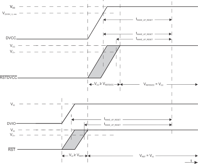
The device remains in reset based on the conditions of the RSTDVCC and RST pins and the voltage present on DVCC voltage supply. If RSTDVCC or RST is held at a logic low or if DVCC is below the SVSH_+ minimum threshold, the device remains in its reset condition; that is, these conditions form a logical OR with respect to device reset. Figure 5-3 Maximum System Frequency