ZHCSE41C August 2015 – May 2017 LP8861-Q1
PRODUCTION DATA.
- 1 特性
- 2 应用
- 3 说明
- 4 修订历史记录
- 5 器件比较表
- 6 Pin Configuration and Functions
-
7 Specifications
- 7.1 Absolute Maximum Ratings
- 7.2 ESD Ratings
- 7.3 Recommended Operating Conditions
- 7.4 Thermal Information
- 7.5 Electrical Characteristics
- 7.6 Internal LDO Electrical Characteristics
- 7.7 Protection Electrical Characteristics
- 7.8 Power Line FET Control Electrical Characteristics
- 7.9 Current Sinks Electrical Characteristics
- 7.10 PWM Brightness Control Electrical Characteristics
- 7.11 Boost/SEPIC Converter Characteristics
- 7.12 Logic Interface Characteristics
- 7.13 Typical Characteristics
-
8 Detailed Description
- 8.1 Overview
- 8.2 Functional Block Diagram
- 8.3 Feature Description
- 8.4 Device Functional Modes
-
9 Application and Implementation
- 9.1 Application Information
- 9.2 Typical Applications
- 10Power Supply Recommendations
- 11Layout
- 12器件和文档支持
- 13机械、封装和可订购信息
8.3.6.1 Adaptive Boost Control and Functionality of LED Fault Comparators
Adaptive boost control function adjusts the boost output voltage to the minimum sufficient voltage for proper LED current sink operation. The output with highest VF LED string is detected and boost output voltage adjusted accordingly. Boost adaptive control voltage step size is defined by maximum boost voltage settings, VSTEP = (VMAX BOOST - VMIN BOOST) / 256. Periodic down pressure is applied to the target boost voltage to achieve better system efficiency.
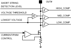
Every LED current sink has 3 comparators for an adaptive boost control and fault detection. Comparator outputs are filtered, filtering time is 1 µs.
 Figure 14. Comparators for Adaptive Voltage Control and LED Fault Detection
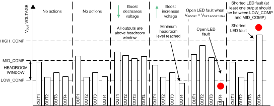
 Figure 15 illustrates different cases which cause boost voltage increase, decrease, or generate faults. In normal operation, voltage at all the OUT# pins is between LOW_COMP and MID_COMP levels and boost voltage stays constant. LOW_COMP level is the minimum for proper LED current sink operation, 1.1 × VSAT + 0.2 V (typical). MID_COMP level is 1.1 × VSAT + 1.2 V (typical) — that is, typical headroom window is 1 V.
When voltage at all the OUT# pins increases above MID_COMP level, boost voltage adapts downwards.
When voltage at any of the OUT# pins falls below LOW_COMP threshold, boost voltage adapts upwards. In the condition where boost voltage reaches the maximum and there are one or more outputs still below LOW_COMP level, an open LED fault is detected.
HIGH_COMP level, 6 V typical, is the threshold for shorted LED detection. When the voltage of one or more of the OUT# pins increases above HIGH_COMP level and at least one of the other outputs is within the normal headroom window, shorted LED fault is detected.
 Figure 15. Boost Adaptation and LED Protection Algorithms