SNVS458D June 2007 – October 2016 LP55281
PRODUCTION DATA.
- 1 Features
- 2 Applications
- 3 Description
- 4 Revision History
- 5 Pin Configuration and Functions
- 6 Specifications
- 7 Detailed Description
- 8 Application and Implementation
- 9 Power Supply Recommendations
- 10Layout
- 11Device and Documentation Support
- 12Mechanical, Packaging, and Orderable Information
6 Specifications
6.1 Absolute Maximum Ratings
over operating free-air temperature range (unless otherwise noted)(1)(2)(3)| MIN | MAX | UNIT | ||
|---|---|---|---|---|
| V (SW, FB, R1-4, G1-4, B1-4, ALED)(4) (5) | –0.3 | 7.2 | V | |
| VVDD1, VVDD2, VVDDIO, VVDDA | –0.3 | 6 | V | |
| Voltage on ASE1-2, IRT, IRGB, VREF | –0.3 to VVDD1 + 0.3 V with 6 V maximum | |||
| Voltage on logic pins | –0.3 to VVDDIO + 0.3 V with 6 V maximum | |||
| V (all other pins): voltage to GND | –0.3 | 6 | ||
| I (VREF) | 10 | µA | ||
| I (R1-4, G1-4, B1-4) | 100 | mA | ||
| Continuous power dissipation(6) | Internally limited | |||
| Junction temperature, TJ-MAX | 150 | °C | ||
| Storage temperature, Tstg | –65 | 150 | °C | |
(1) Stresses beyond those listed under Absolute Maximum Ratings may cause permanent damage to the device. These are stress ratings only, which do not imply functional operation of the device at these or any other conditions beyond those indicated under Recommended Operating Conditions. Exposure to absolute-maximum-rated conditions for extended periods may affect device reliability.
(2) All voltages are with respect to the potential at the GND pins.
(3) If Military/Aerospace specified devices are required, contact the Texas Instruments Sales Office/ Distributors for availability and specifications.
(4) Battery/Charger voltage must be above 6 V, and no more than 10% of the operational lifetime.
(5) Voltage tolerance of LP55281 above 6 V relies on fact that VVDD1 and VVDD2 (2.8 V) are available (ON) at all conditions. If VVDD1 and VVDD2 are not available (ON) at all conditions, Texas Instruments does not ensure any parameters or reliability for this device.
(6) Internal thermal shutdown circuitry protects the device from permanent damage. Thermal shutdown engages at TJ = 160°C (typical) and disengages at TJ = 140°C (typical)
6.2 ESD Ratings
| VALUE | UNIT | |||
|---|---|---|---|---|
| V(ESD) | Electrostatic discharge | Human-body model (HBM), per ANSI/ESDA/JEDEC JS-001(1) | ±2000 | V |
(1) JEDEC document JEP155 states that 500-V HBM allows safe manufacturing with a standard ESD control process..
6.3 Recommended Operating Conditions
over operating free-air temperature range (unless otherwise noted)(1)(2)| MIN | NOM | MAX | UNIT | ||
|---|---|---|---|---|---|
| V (SW, FB, R1-4, G1-4, B1-4, ALED) | 0 | 6 | V | ||
| VVDD1,2 with external LDO | 2.7 | 5.5 | V | ||
| VVDD1,2 with internal LDO | 3 | 5.5 | V | ||
| VDDA | 2.7 | 2.9 | V | ||
| VVDDIO | 1.65 | VVDD1 | |||
| Voltage on ASE1-2 | 0.1 V to VVDDA – 0.1 V | ||||
| Recommended load current | 0 | 300 | mA | ||
| Junction temperature, TJ | –30 | 125 | °C | ||
| Ambient temperature, TA (2) | –30 | 85 | °C | ||
(1) All voltages are with respect to the potential at the GND pins.
(2) In applications where high power dissipation and/or poor package thermal resistance is present, the maximum ambient temperature may have to be derated. Maximum ambient temperature (TA-MAX) is dependent on the maximum operating junction temperature (TJ-MAX-OP = 125°C), the maximum power dissipation of the device in the application (PD-MAX), and the junction-to-ambient thermal resistance of the part/package in the application (RθJA), as given by the following equation: TA-MAX = TJ-MAX-OP – (RθJA x PD-MAX).
6.4 Thermal Information
| THERMAL METRIC(1) | LP55281 | UNIT | ||
|---|---|---|---|---|
| YPG (DSGBA) | YZR (DSGBA) | |||
| 36 PINS | 36 PINS | |||
| RθJA | Junction-to-ambient thermal resistance | 48.9 | 49.1 | °C/W |
| RθJC(top) | Junction-to-case (top) thermal resistance | 0.2 | 0.2 | °C/W |
| RθJB | Junction-to-board thermal resistance | 10.6 | 10.8 | °C/W |
| ψJT | Junction-to-top characterization parameter | 0.1 | 0.1 | °C/W |
| ψJB | Junction-to-board characterization parameter | 10.4 | 10.6 | °C/W |
(1) For more information about traditional and new thermal metrics, see Semiconductor and IC Package Thermal Metrics.
6.5 Electrical Characteristics
Unless otherwise noted, specifications apply to Functional Block Diagram with: VVDD1 = VVDD2 = 3.6 V, VVDDIO = 2.8 V, CVDD = CVDDIO = 100 nF, COUT = CIN = 10 µF, CVDDA= 1 µF, CREF = 100 nF, L1 = 4.7 µH, RRGB = 8.2 kΩ and RRT = 82 kΩ, and limits are for TJ = 25°C.(1)(2) (3).| PARAMETER | TEST CONDITIONS | MIN | TYP | MAX | UNIT | |
|---|---|---|---|---|---|---|
| IVDD | Standby supply current (VDD1 + VDD2 + leakage to SW, FB, RGB1-4, ALED) | NSTBY = L SCK = SS = SI = H NRST = L |
1 | µA | ||
| NSTBY = L SCK = SS = SI = H NRST = L –30°C < TA < 85°C |
10 | |||||
| No-boost supply current (VDD1 + VDD2) | NSTBY = H, EN_BOOST = L SCK = SS = SI = H Audio synchronization and LEDs OFF |
350 | µA | |||
| No-load supply current (VDD1 + VDD2) | NSTBY = H, EN_BOOST = H, SCK = SS = SI = H Audio synchronization and LEDs OFF Autoload OFF |
0.6 | mA | |||
| Total RGB drivers quiescent current (VDD1 + VDD2) | EN_RGBx = H | 250 | µA | |||
| ALED driver current (VDD1 + VDD2) | ALED[7:0] = FFh | 180 | µA | |||
| ALED[7:0] = 00h | 0 | µA | ||||
| Audio synchronization current (VDD1 + VDD2) | Audio synchronization ON VDD1,2 = 2.8 V |
390 | µA | |||
| Audio synchronization ON VDD1,2 = 3.6 V |
700 | µA | ||||
| IDDIO | VDDIO standby supply current | NSTBY = L SCK = SS = SI = H –30°C < TA < 85°C |
1 | µA | ||
| VDDIO supply current | 1 MHz SCK frequency in SPI modeCL = 50 pF at SO pin | 20 | µA | |||
| VDDA | Output voltage of internal LDO for analog parts | See(4) | –3% | 2.8 | 3% | V |
| MAGNETIC BOOST DC-DC CONVERTER ELECTRICAL CHARACTERISTICS | ||||||
| ILOAD | Recommended load current | 3 V ≤ VIN
VOUT = 5 V |
0 | 300 | mA | |
| 3 V ≤ VIN
VOUT = 4 V |
0 | 400 | mA | |||
| VOUT | Output voltage accuracy (FB pin) |
3 V ≤ VIN ≤ VOUT – 0.5 V VOUT = 5 V –30°C < TA < 85°C |
–5% | 5% | ||
| Output voltage (FB pin) | 1 mA ≤ ILOAD ≤ 300 mA VIN > VOUT + VSchottky(5) |
VIN – VSchottky | V | |||
| RDSON | Switch ON resistance | VDD1,2 = 3 V, ISW = 0.5 A | 0.4 | Ω | ||
| VDD1,2 = 3 V, ISW = 0.5 A –30°C < TA < 85°C |
0.8 | |||||
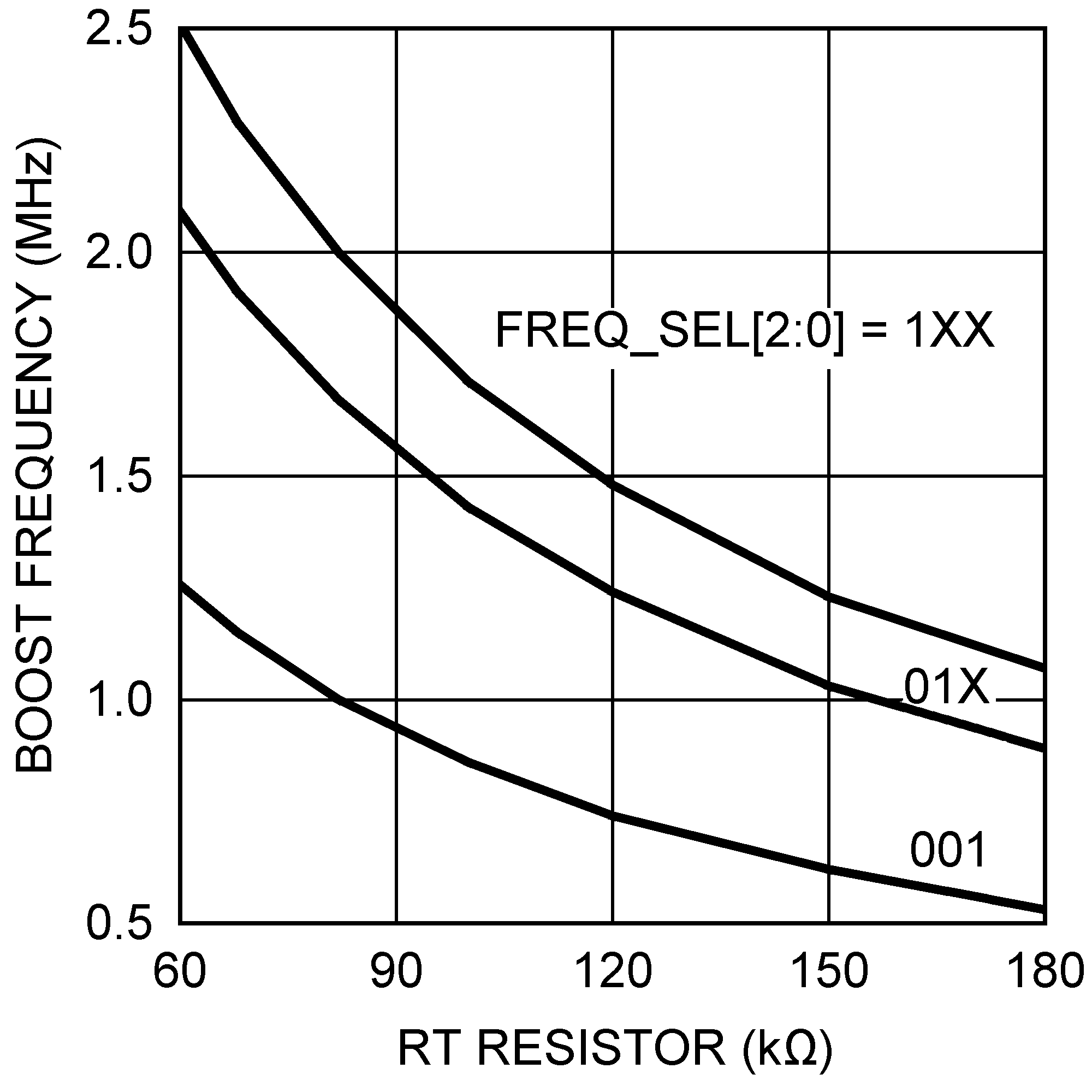
| fBoost | PWM mode switching frequency | RT = 82 kΩ freq_sel[2:0] = 1XX |
2 | MHz | ||
| Frequency accuracy | 2.7 V ≤ VDDA ≤ 2.9 V RT = 82 kΩ ± 1% |
–7% | ±3% | 7% | ||
| 2.7 V ≤ VDDA ≤ 2.9 V RT = 82 kΩ ± 1% –30°C < TA < 85°C |
–10% | 10% | ||||
| tPULSE | Switch pulse minimum width | no load | 30 | ns | ||
| tSTART-UP | Start-up time | Boost start-up from STANDBY(6) | 10 | ms | ||
| ISW_MAX | SW pin current limit | 700 | 800 | 900 | mA | |
| –30°C < TA < 85°C | 550 | 950 | ||||
| RGB DRIVER ELECTRICAL CHARACTERISTICS (R1-4, G1-4, B1-4) | ||||||
| Ileakage | R1-4, G1-4, B1-4 pin leakage current | 5.5 V at measured pin | 0.1 | µA | ||
| 5.5 V at measured pin –30°C < TA < 85°C |
1 | |||||
| IRGB | Maximum recommended sink current | Limited with external resistor RRGB
–30°C < TA < 85°C |
40 | mA | ||
| Accuracy at 15 mA | RRGB = 8.2 kΩ ± 1% | ±5% | ||||
| Current mirror ratio | See(6) | 1 : 100 | ||||
| RGB1-4 current mismatch | IRGB = 15 mA | ±5% | ||||
| fPWM | RGB switching frequency | Accuracy defined by internal oscillator, frequency value selectable | fPWM | |||
| AUDIO SYNCHRONIZATION INPUT ELECTRICAL CHARACTERISTICS | ||||||
| ZIN | Input Impedance of ASE1, ASE2 | See(6) | 10 | 15 | kΩ | |
| AIN | ASE1, ASE2 audio input level range (peak-to-peak) | Min input level needs maximum gain; Max input level for minimum gain | 0 | 1600 | mV | |
| ALED DRIVER ELECTRICAL CHARACTERISTICS | ||||||
| Ileakage | Leakage current | VALED = 5.5 V | 0.03 | µA | ||
| VALED = 5.5 V –30°C < TA < 85°C |
1 | |||||
| IALED | ALED current tolerance | IALED set to 13.2 mA | 13.2 | mA | ||
| IALED set to 13.2 mA –30°C < TA < 85°C |
11.9 | 14.5 | mA | |||
| –10% | 10% | |||||
| LOGIC INTERFACE CHARACTERISTICS | ||||||
| VIL | Input low level | –30°C < TA < 85°C | 0.2 × VDDIO | V | ||
| VIH | Input high level | –30°C < TA < 85°C | 0.8 × VDDIO | V | ||
| II | Logic input current | –30°C < TA < 85°C | –1 | 1 | µA | |
| fSCK/SCL | Clock frequency | I2C, –30°C < TA < 85°C | 400 | kHz | ||
| –30°C < TA < 85°C SPI mode, VDDIO > 1.8 V |
13 | MHz | ||||
| –30°C < TA < 85°C SPI mode, 1.65V ≤ VDDIO < 1.8V |
5 | MHz | ||||
| LOGIC INPUT NRST | ||||||
| VIL | Input low level | –30°C < TA < 85°C | 0.5 | V | ||
| VIH | Input high level | –30°C < TA < 85°C | 1.2 | V | ||
| II | Logic input current | –30°C < TA < 85°C | –1 | 1 | µA | |
| tNRST | Reset pulse width | –30°C < TA < 85°C | 10 | µs | ||
| LOGIC OUTPUT SO | ||||||
| VOL | Output low level | ISO = 3 mA VDDIO > 1.8 V | 0.3 | V | ||
| ISO = 3 mA VDDIO > 1.8 V –30°C < TA < 85°C |
0.5 | |||||
| ISO = 2 mA, 1.65V ≤ VDDIO < 1.8 V | 0.3 | |||||
| ISO = 2 mA, 1.65V ≤ VDDIO < 1.8 V –30°C < TA < 85°C |
0.5 | |||||
| VOH | Output high level | ISO = –3 mA, VDDIO > 1.8 V | VDDIO – 0.3 | V | ||
| ISO = –3 mA, VDDIO > 1.8 V –30°C < TA < 85°C |
VDDIO – 0.5 | |||||
| ISO = –2 mA, 1.65V ≤ VDDIO < 1.8 V | VDDIO – 0.3 | |||||
| ISO = –2 mA, 1.65V ≤ VDDIO < 1.8 V –30°C < TA < 85°C |
VDDIO – 0.5 | |||||
| IL | Output leakage current | VSO = 2.8 V, –30°C < TA < 85°C | 1 | µA | ||
| LOGIC OUTPUT SDA | ||||||
| VOL | Output low level | ISDA = 3 mA | 0.3 | V | ||
| ISDA = 3 mA, –30°C < TA < 85°C | 0.5 | |||||
(1) All voltages are with respect to the potential at the GND pins.
(2) Minimum (MIN) and maximum (MAX) limits are ensured by design, test or statistical analysis. Typical (TYP) numbers are not ensured, but do represent the most likely norm.
(3) Low-ESR surface-mount ceramic capacitors (MLCCs) used in setting electrical characteristics.
(4) VDDA output is not recommended for external use.
(5) When VIN rises above VOUT + VSchottky, VOUT starts to follow the VIN voltage rise so that VOUT = VIN – VSchottky.
(6) Data ensured by design.
6.6 SPI Timing Requirements
VDD = VDDIO = 2.8 V(1)| MIN | MAX | UNIT | ||
|---|---|---|---|---|
| 1 | Cycle time | 70 | ns | |
| 2 | Enable lead time | 35 | ns | |
| 3 | Enable lag time | 35 | ns | |
| 4 | Clock low time | 35 | ns | |
| 5 | Clock high time | 35 | ns | |
| 6 | Data setup time | 20 | ns | |
| 7 | Data hold time | 0 | ns | |
| 8 | Data access time | 20 | ns | |
| 9 | Disable time | 10 | ns | |
| 10 | Data valid | 20 | ns | |
| 11 | Data hold time | 0 | ns | |
(1) Data ensured by design.
 Figure 1. SPI Timing Diagram
6.7 I2C Timing Requirements
VDD1,2 = 3 V to 4.5 V, VDDIO = 1.65 V to VDD1,2 (1)| MIN | MAX | UNIT | ||
| 1 | Hold time (repeated) START condition | 0.6 | µs | |
| 2 | Clock low time | 1.3 | µs | |
| 3 | Clock high time | 600 | ns | |
| 4 | Setup time for a repeated START Condition | 600 | ns | |
| 5 | Data hold time | 50 | ns | |
| 6 | Data setup time | 100 | ns | |
| 7 | Rise time of SDA and SCL | 20 + 0.1Cb | 300 | ns |
| 8 | Fall time of SDA and SCL | 15 + 0.1Cb | 300 | ns |
| 9 | Set-up time for STOP condition | 600 | ns | |
| 10 | Bus free time between a STOP and a START condition | 1.3 | µs | |
| Cb | Capacitive load for each bus line | 10 | 200 | pF |
(1) Data ensured by design.
 Figure 2. I2C Timing Diagram
6.8 Boost Converter Typical Characteristics
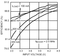
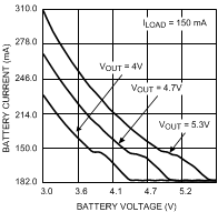
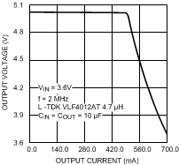
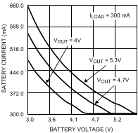
6.9 RGB Driver Typical Characteristics
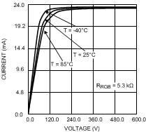 Figure 8. Output Current vs Pin Voltage
 (Current Sink Mode)
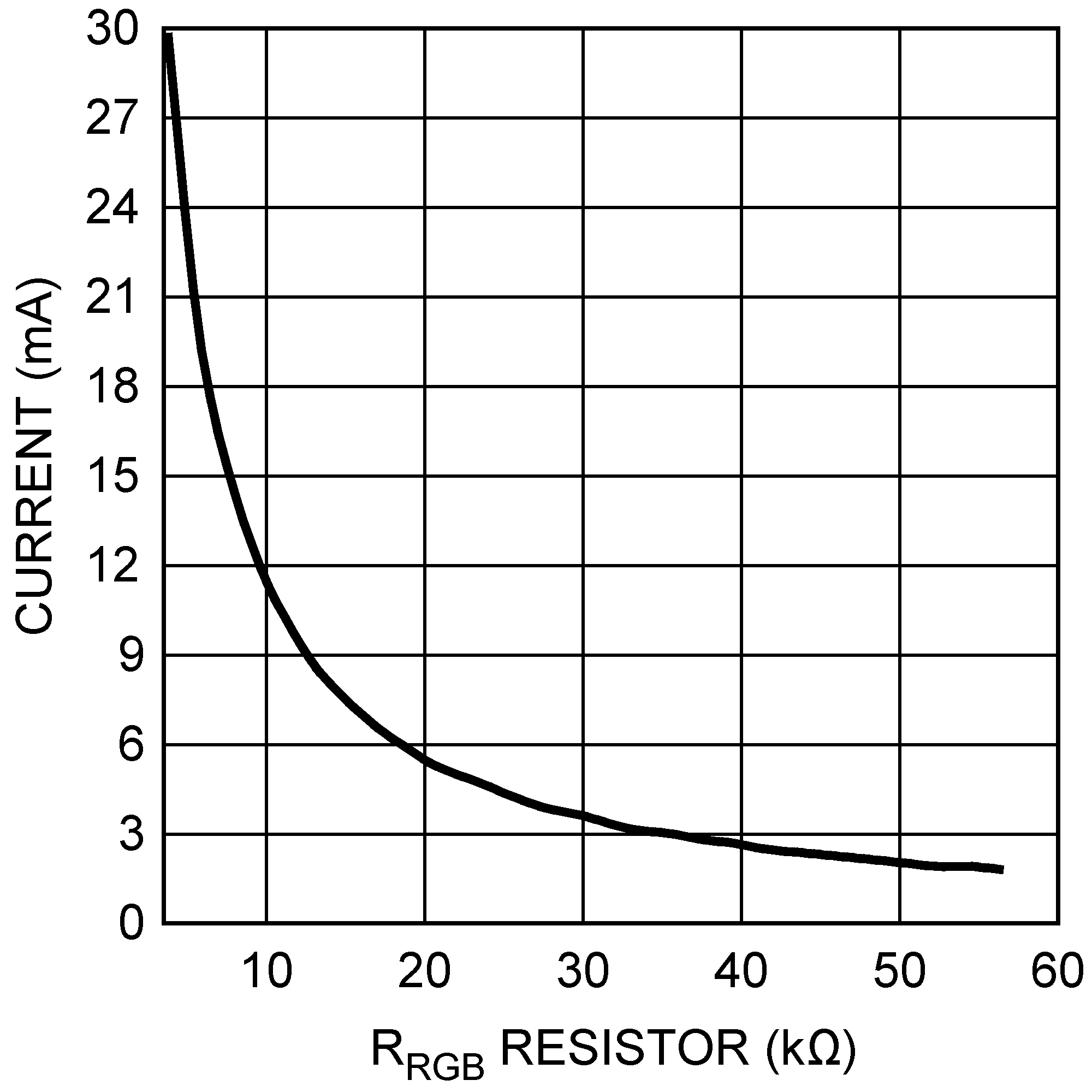
(Current Sink Mode)