SNVS458D June 2007 – October 2016 LP55281
PRODUCTION DATA.
- 1 Features
- 2 Applications
- 3 Description
- 4 Revision History
- 5 Pin Configuration and Functions
- 6 Specifications
- 7 Detailed Description
- 8 Application and Implementation
- 9 Power Supply Recommendations
- 10Layout
- 11Device and Documentation Support
- 12Mechanical, Packaging, and Orderable Information
8 Application and Implementation
NOTE
Information in the following applications sections is not part of the TI component specification, and TI does not warrant its accuracy or completeness. TI’s customers are responsible for determining suitability of components for their purposes. Customers should validate and test their design implementation to confirm system functionality.
8.1 Application Information
The LP55281 quadruple RGB driver with integrated boost converter provides a complete solution for driving up to 12 LEDs via either I2C or SPI interface.
8.2 Typical Application
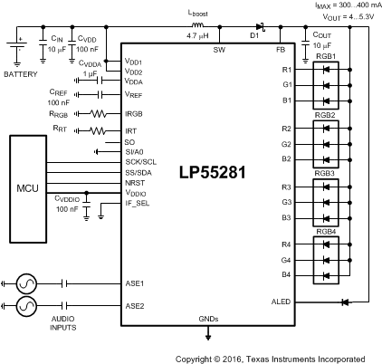 Figure 26. LP55281 Typical Application
8.2.1 Design Requirements
For typical LED-driver applications, use the parameters listed in Table 10.
Table 10. Design Parameters
| DESIGN PARAMETER | EXAMPLE VALUE |
|---|---|
| Input voltage | 3 V |
| Output voltage | 5 V |
| SW pin current limit | 550 mA (minimum) |
| Efficiency | 75% |
8.2.2 Detailed Design Procedure
The output current can be approximated by using this formula: IOUT = (VIN × ISW_MAX × efficiency) / VOUT.
Example: 3 V × 550 mA × 0.75 / 5 V = 248 mA
8.2.2.1 Recommended External Components
8.2.2.1.1 Output Capacitor, COUT
The output capacitor COUT directly affects the magnitude of the output ripple voltage. In general, the higher the value of COUT, the lower the output ripple magnitude. Multilayer ceramic capacitors with low ESR are the best choice. At the lighter loads, the low ESR ceramics offer a much lower VOUT ripple than the higher ESR tantalums of the same value. At the higher loads, the ceramics offer a slightly lower VOUT ripple magnitude than the tantalums of the same value. However, the dv/dt of the VOUT ripple with the ceramics is much lower than the tantalums under all load conditions. Capacitor voltage rating must be sufficient, TI recommends 10 V or greater.
Some ceramic capacitors, especially those in small packages, exhibit a strong capacitance reduction with the increased applied voltage. The capacitance value can fall to below half of the nominal capacitance. Output capacitance that is too low increase the noise, and it can make the boost converter unstable.
8.2.2.1.2 List Of Recommended External Components
| PARAMETER | VALUE | UNIT | TYPE | |
| CVDD1 | C between VDD1 and GND | 100 | nF | Ceramic, X7R/X5R |
| CVDD2 | C between VDD2 and GND | 100 | nF | Ceramic, X7R/X5R |
| CVDDIO | C between VDDIO and GND | 100 | nF | Ceramic, X7R/X5R |
| CVDDA | C between VDDA and GND | 1 | µF | Ceramic, X7R/X5R |
| COUT | C between FB and GND | 10 | µF | Ceramic, X7R/X5R |
| CIN | C between battery voltage and GND | 10 | µF | Ceramic, X7R/X5R |
| LBOOST | L between SW and VBAT at 2 MHz | 4.7 | µH | Shielded, low ESR, ISAT 1A |
| CVREF | C between VREF and GND | 100 | nF | Ceramic, X7R |
| CVDDIO | C between VDDIO and GND | 100 | nF | Ceramic, X7R |
| RRGB | R between IRGB and GND | 8.2 | kΩ | ±1% |
| RRT | R between IRT and GND | 82 | kΩ | ±1% |
| D1 | Rectifying Diode (Vf at maxload) | 0.3 | V | Schottky diode |
| CASE | C between Audio input and ASEx | 100 | nF | Ceramic, X7R/X5R |
| LEDs | User defined | |||
8.2.2.1.3 Input Capacitor, CIN
The input capacitor CIN directly affects the magnitude of the input ripple voltage and to a lesser degree the VOUT ripple. A higher value CIN gives a lower VIN ripple. Capacitor voltage rating must be sufficient, TI recommends 10 V or greater.
8.2.2.1.4 Output Diode, D1
A Schottky diode must be used for the output diode. To maintain high efficiency the average current rating of the Schottky diode must be larger than the peak inductor current (1 A). Schottky diodes with a low forward drop and fast switching speeds are ideal for increasing efficiency in portable applications. Choose a reverse breakdown of the Schottky diode larger than the output voltage. Do not use ordinary rectifier diodes, since slow switching speeds and long recovery times cause the efficiency and the load regulation to suffer.
8.2.2.1.5 Inductor, L
The high switching frequency of the LP55281 device enables the use of the small surface mount inductor. A 4.7-µH shielded inductor is suggested for 2-MHz operation, use 10 µH at 1 MHz. The inductor should have a saturation current rating higher than the peak current it will experience during circuit operation (approximately 1 A). Less than 300-mΩ ESR is suggested for high efficiency. Open core inductors cause flux linkage with circuit components and interfere with the normal operation of the circuit. This should be avoided. For high efficiency, choose an inductor with a high frequency core material such as ferrite to reduce the core losses. To minimize radiated noise, use a toroid, pot core or shielded core inductor. TI recommends inductors LPS3015 and LPS4012 from Coilcraft and VLF4012 from TDK.
8.2.3 Application Curves
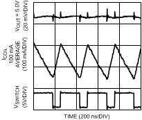
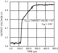
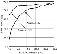
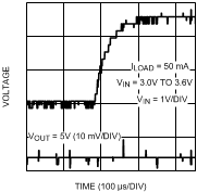
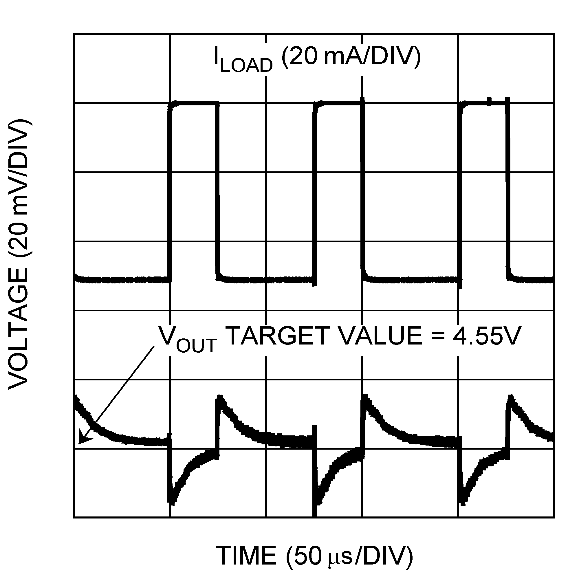
| 50 - 100 mA |
8.3 Initialization Set Up Example
The following table gives an example initialization sequence to illustrate the various LED and Boost configuration options. Not every feature of the LP55281 is configured in this example.
Table 11. Initialization Example
| ADDRESS | DATA | REGISTER | COMMENT | |
|---|---|---|---|---|
| 60h | 00h | RESET | Execute software reset to initialize LP55281 | |
| 00h | 3Fh | RED 1 | IPLS = 0 (25% IRGB), PWM = 100% | |
| 01h | 5Fh | GREEN1 | IPLS = 1 (50% IRGB), PWM = 50% | |
| 02h | 90h | BLUE1 | IPLS = 2 (75% IRGB), PWM = 25.4% | |
| 03h | C8h | RED 2 | IPLS = 3 (100% IRGB), PWM = 12.7% | |
| 04h | 1Fh | GREEN2 | IPLS = 0 (25% IRGB), PWM = 50% | |
| 05h | 10h | BLUE2 | IPLS = 0 (25% IRGB), PWM = 25.4% | |
| 06h | 07h | RED 3 | IPLS = 0 (25% IRGB), PWM = 11.1% | |
| 07h | 03h | GREEN3 | IPLS = 0 (25% IRGB), PWM = 4.8% | |
| 08h | 01h | BLUE3 | IPLS = 0 (25% IRGB), PWM = 1.6% | |
| 09h | 0h | RED 4 | IPLS = 0 (25% IRGB), PWM = 0% | |
| 0Ah | 0h | GREEN4 | IPLS = 0 (25% IRGB), PWM = 0% | |
| 0Bh | 0h | BLUE4 | IPLS = 0 (25% IRGB), PWM = 0% | |
| 0Fh | 0Fh | Boost Output | Boost output voltage set to 4.7V | |
| 10h | 07h | Frequency Selections | PWM frequency (FPWM[1:0] = 0, 9.92 kHz), Boost SW frequency = 2 MHz | |
| 11h | CFh | Enables | NSTBY, EN_BOOST, EN_RGB4, EN_RGB3, EN_RGB2, EN_RGB1 = 1 (exit standby state, enable boost and rgb drivers) | |