SNVS500C July 2007 – November 2016 LP5524
PRODUCTION DATA.
8 Application and Implementation
NOTE
Information in the following applications sections is not part of the TI component specification, and TI does not warrant its accuracy or completeness. TI’s customers are responsible for determining suitability of components for their purposes. Customers should validate and test their design implementation to confirm system functionality.
8.1 Application Information
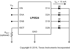
The LP5524 device provides an easy-to-use solution for driving up to 4 indicator LEDs.
8.2 Typical Application
 Figure 5. LP5524 Typical Application
8.2.1 Design Requirements
For typical LED-driver applications, use the parameters listed in Table 1.
Table 1. Design Parameters
| DESIGN PARAMETER | EXAMPLE VALUE |
|---|---|
| Minimum input voltage | 2.7 V |
| ISET resistance | 34 kΩ |
| Output current | 60 mA |
| Maximum LED Vƒ | 2.625 V |
8.2.2 Detailed Design Procedure
8.2.2.1 Recommended External Components
8.2.2.1.1 Input Capacitor, CIN
Although not required for normal operation, a capacitor can be added to VIN to reduce line noise. TI recommends using a surface-mount multi-layer ceramic capacitor (MLCC). MLCCs with a X7R or X5R temperature characteristic are preferred.
Table 2. List Of Recommended External Components
| PARAMETER | VALUE | UNIT | TYPE | |
|---|---|---|---|---|
| CIN | VDD bypass capacitor | 100 | nF | Ceramic, X7R or X5R |
| RISET | Current set resistor for 15.9-mA LED current | 32.4 | kΩ | 1% |
| LEDs | User defined | |||
8.2.2.1.2 Current Set Resistor, RISET
If other than 5 mA current is required, RISET resistor can be used to adjust the current. For a 15.9-mA current a 32.4 kΩ resistor is required. Accuracy of the resistor directly effects to the accuracy of the LED current. TI recommends accuracy of 1% or better.
Table 3. Recommended E96 Series (1% Tolerance) Current Set Resistors
| RISET (kΩ) | IDX (mA) | RISET (kΩ) | IDX (mA) |
| 169 | 3.0 | 34.0 | 15.1 |
| 127 | 4.1 | 32.4 | 15.9 |
| 102 | 5.0 | 30.1 | 17.1 |
| 84.5 | 6.1 | 28.7 | 17.9 |
| 73.2 | 7.0 | 26.7 | 19.3 |
| 64.9 | 7.9 | 25.5 | 20.2 |
| 56.2 | 9.2 | 24.3 | 21.2 |
| 51.1 | 10.1 | 23.2 | 22.2 |
| 46.4 | 11.1 | 22.1 | 23.3 |
| 42.2 | 12.2 | 21.5 | 24.0 |
| 39.2 | 13.1 | 20.5 | 25.1 |
| 36.5 | 14.1 |
8.2.3 Application Curves

