SNVS179F February 2003 – September 2015 LP3995
PRODUCTION DATA.
- 1 Features
- 2 Applications
- 3 Description
- 4 Revision History
- 5 Pin Configuration and Functions
- 6 Specifications
- 7 Parameter Measurement Information
- 8 Detailed Description
- 9 Application and Implementation
- 10Power Supply Recommendations
- 11Layout
- 12Device and Documentation Support
- 13Mechanical, Packaging, and Orderable Information
5 Pin Configuration and Functions
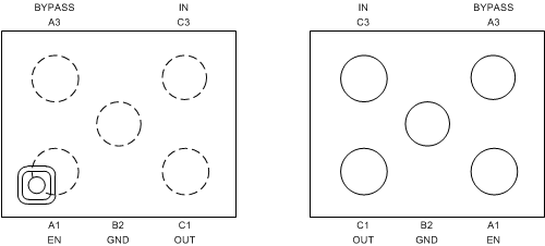
YZR Package
5-Pin DSBGA
Top View

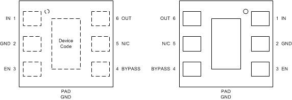
NGD Package
6-Pin WSON
Top View

Pin Functions
| PIN | TYPE | DESCRIPTION | ||
|---|---|---|---|---|
| NAME | WSON | DSBGA | ||
| BYPASS | 4 | A3 | — | Bypass capacitor connection. Connect a 0.01-µF capacitor for noise reduction. |
| EN | 3 | A1 | Input | Enable input; Disables the regulator when ≤ 0.4 V. Enables the regulator when ≥ 0.9 V. |
| GND | 2 | B2 | Ground | Common ground |
| GND | Thermal Pad | — | Ground | The exposed thermal pad on the bottom of the WSON package should be connected to a copper thermal pad on the PCB under the package. The use of thermal vias to remove heat from the package into the PCB is recommended. Connect the exposed thermal pad to ground potential or leave floating. Do not connect the thermal pad to any potential other than the same ground potential seen at device pin 2. For additional information on using TI's non pull-back WSON package, see TI Application Note AN- 1187 Leadless Leadframe Package (LLP) (SNOA401). |
| IN | 1 | C3 | Input | Voltage supply input |
| N/C | 5 | — | — | No internal connection. This pin can be connected to GND, or left open. |
| OUT | 6 | C1 | Output | Voltage output. Connect this output to the load circuit. |